The advanced packaging revolution is creating a PCB substrate boom in 2026, with the global ABF substrate market reaching $7.19 billion and substrate-like PCB (SLP) demand hitting $4.24 billion. As TSMC, Intel, and Amkor race to expand packaging capacity, the ripple effects are transforming every layer of the electronics supply chain — from raw substrate materials to finished PCBA assemblies.
The Packaging Bottleneck Is the New Chip Bottleneck
For years, the semiconductor industry focused on shrinking transistor nodes. In 2026, the real constraint has shifted upstream: advanced packaging. CNBC reported in April that "even the best chips made in the U.S. take a round trip to Taiwan" for packaging, underscoring how critical this capability has become.
TSMC is expected to report a fourth consecutive quarter of record earnings in Q1 2026, with net profit surging 50% year-over-year driven by insatiable AI demand. But packaging capacity — not wafer fabrication — is increasingly the gating factor for NVIDIA's GB200, AMD's MI400, and custom AI accelerators from hyperscalers.
Intel's landmark $25 billion partnership with Elon Musk's Terafab project further validates this shift. The deal positions Intel as a foundry partner for advanced packaging and chip production for AI and robotics applications, adding credible long-term demand to Intel's packaging revenue pipeline.
ABF Substrates: The $7.19 Billion Engine
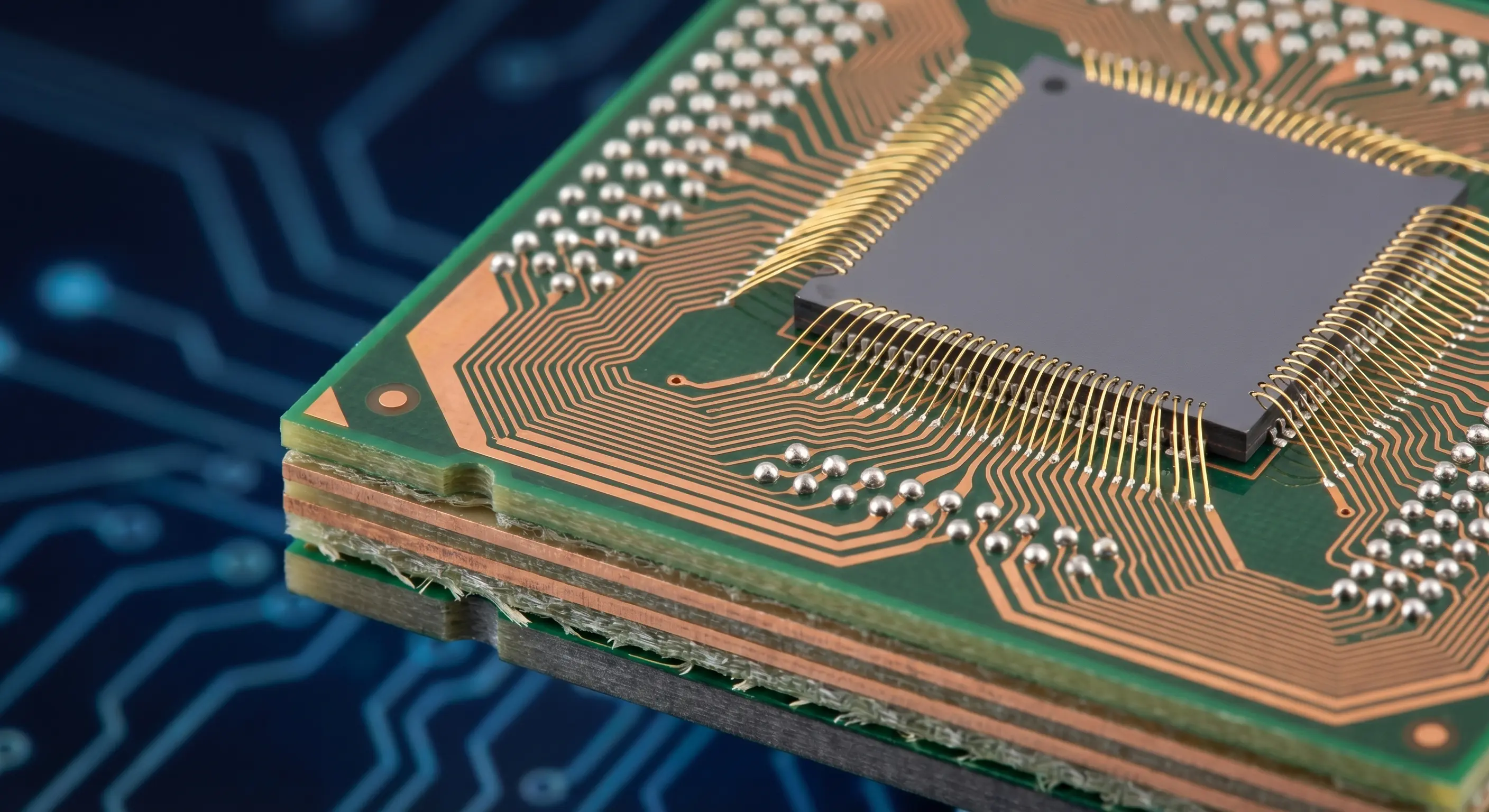
Ajinomoto Build-up Film (ABF) substrates — the unsung heroes of modern chip packaging — are experiencing explosive growth. Market research values the global ABF substrate market at $7.19 billion in 2026, projected to reach $13.95 billion by 2035 at a 6.9% CAGR.
ABF substrates are essential for:
- CPU and GPU packages — High-density interconnects for AI training and inference chips
- Server chipsets — Intel, AMD, and ARM-based data center processors
- High-performance networking — 800G and 1.6T optical interconnect modules
- Automotive ADAS — Advanced driver-assistance systems requiring complex multi-die packaging
The challenge? ABF substrate supply remains concentrated among a handful of Japanese, Korean, and Taiwanese manufacturers. Unimicron, Ibiden, Kinsus, and Shennan Circuits control over 70% of global capacity, creating strategic supply chain vulnerabilities for Western OEMs.
Substrate-Like PCBs: Bridging the Gap at $4.24 Billion
As advanced packaging demands push traditional PCB technology to its limits, substrate-like PCBs (SLP) have emerged as the critical bridge technology. The SLP market is valued at $4.24 billion in 2026, growing at a 7.37% CAGR to reach $6.05 billion by 2031, according to Mordor Intelligence.
SLP technology enables line-and-space geometries below 25μm — approaching semiconductor substrate territory — while maintaining the cost structure and scalability of PCB manufacturing. This makes SLP the go-to solution for:
- AI edge devices — Wearables, IoT gateways, and on-device inference modules
- 5G/6G RF modules — Millimeter-wave antenna-in-package designs
- Miniaturized consumer electronics — Foldable phones, AR glasses, hearables
- Medical implants — Ultra-compact, high-reliability assemblies
The modified semi-additive process (mSAP) that enables SLP production is now being adopted by leading PCB fabricators worldwide, but the technical门槛 remains high — requiring laser direct imaging, controlled impedance stackups, and advanced plating capabilities.
Victory Giant's IPO Signals Market Confidence
The advanced packaging PCB boom is also creating major winners. Victory Giant Technology — the world's #1 supplier of AI/HPC PCBs in H1 2025 — launched its Hong Kong IPO in April 2026 with revenue of RMB 19.3 billion and net profit surging 273%. The company's dominance in AI server and HPC PCB manufacturing demonstrates how specialized PCB capabilities are being rewarded by capital markets.
According to Frost & Sullivan, Victory Giant's global market share in AI/HPC PCBs exceeds the combined share of the next three competitors, highlighting the winner-take-most dynamics of this specialized segment.
SEMI Data: $135 Billion Equipment Spend in 2025
The upstream investment tells the story. SEMI reported that global semiconductor manufacturing equipment billings reached $135.1 billion in 2025, up 15% from $117.1 billion in 2024. A significant portion of this investment flows to advanced packaging equipment — including bumping, wafer-level packaging, and panel-level fan-out tools that directly impact PCB substrate demand.
This equipment spending cycle signals sustained multi-year demand for advanced substrates and high-density PCBs, well beyond 2026. For contract manufacturers, the implication is clear: invest in HDI and SLP capabilities now, or risk being shut out of the fastest-growing segments.
What OEMs Should Demand from PCBA Partners
As advanced packaging reshapes PCB requirements, OEMs need manufacturing partners who understand the full chain — from substrate selection to final assembly. Key capabilities to evaluate:
- HDI and SLP experience — Proven production with microvias, mSAP, and fine-line etching
- Advanced materials knowledge — High-Tg, low-Dk/Df laminates for high-speed applications
- Thermal management — Copper coin inserts, embedded heat pipes, and metal-core PCB options
- Substrate sourcing — Relationships with ABF and SLP substrate suppliers to secure allocation
- DFM for packaging — Design review that accounts for warpage, CTE mismatch, and via reliability
- Test coverage — AOI, X-ray, ICT, and functional test for high-density assemblies
Illuminious: Ready for the Substrate Era
Illuminious LLC is positioned at the intersection of advanced packaging demand and global manufacturing capability. With production facilities in Southeast Asia — including Batam's Free Trade Zone — the company offers HDI and SLP-adjacent PCBA services with turnkey integration from design review through volume production.
"The substrate boom isn't just a semiconductor story — it's a PCB story," said an Illuminious spokesperson. "Every advanced package needs an advanced board. Our investment in fine-pitch SMT, microvia capability, and advanced materials sourcing ensures our clients can capitalize on this market shift without supply chain friction."
For OEMs navigating the advanced packaging transition, Illuminious offers the manufacturing depth and supply chain agility to turn market opportunity into delivered product — on time and at scale.