PCB manufacturing: choosing the route for your board
No CAD yet? Our design team can take it from a sketch or a spec.
Walk Shenzhen factories with us, Dec 6–11. See the tour
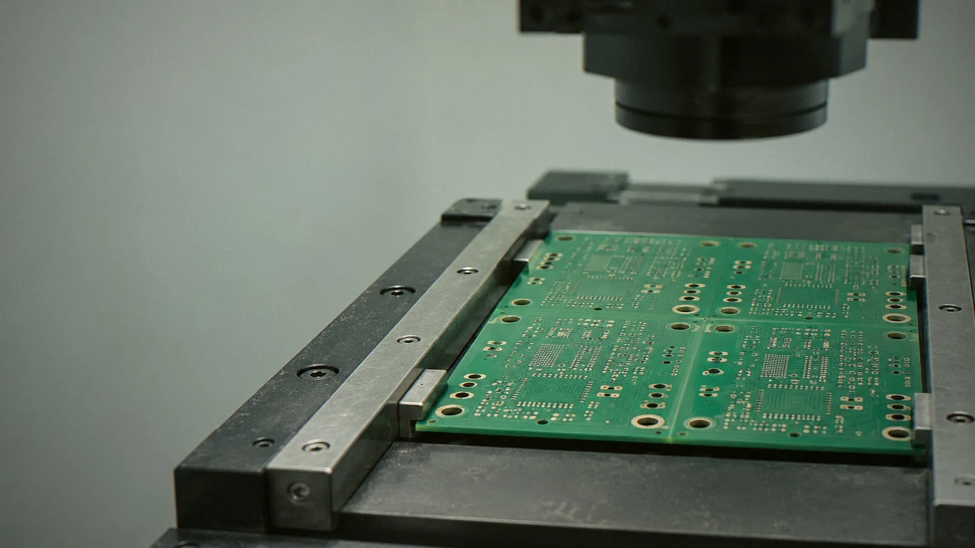
Fabrication turns copper, drill and mask layers into a physical board: laminate is drilled and plated, copper is etched, mask and legend are applied, a finish protects the pads, and the panel is routed and tested. Standard construction fits the standard route. Illuminious is a U.S. NPI engineering company, and we fabricate boards in our own factory after our engineers check the stack-up against how it will be built. Engineered in San Francisco. Prototype builds, DFM and mass production in our own factory in Shenzhen. When the construction itself needs process planning, the board belongs on the advanced route.
Every electronic product needs a board, from a two-layer sensor board to a twelve-layer controller. The real decision is which route to use. The standard route covers FR-4 or aluminum core, up to twelve layers and through-hole vias. Blind, buried or laser microvias, sequential lamination, backdrill, press-fit holes, low-loss or polyimide laminate, copper beyond 3 oz, more than twelve layers, or rigid-flex all go to the advanced route. The difference is not quality. It is how much of the construction a calculator can safely assume.
A simple test sorts the two. If your board has only through-hole vias, twelve layers or fewer, and FR-4 or aluminum, start on the standard route. If any line in your fabrication notes names a microvia, a laminate brand, a backdrill depth or a press-fit hole, start on the advanced route. The free engineering review moves the board if you picked wrong.
What our engineers check in a board package
The free engineering review reads the fabrication package against the configuration you declared. It confirms what a calculator cannot:
- Stack-up. Layer order, dielectric thickness and copper weights that agree with each other and with any impedance targets.
- Drill structure. Via types, aspect ratios and the smallest drill, against the route you chose.
- Feature sizes. The minimum trace, space and annular ring, against the process window.
- Copper balance. Even copper across layers, so the board stays flat through lamination and reflow.
- Panel. Whether the panel suits both fabrication and assembly handling.
- Finish against parts. A flat finish where fine-pitch and BGA parts need it.
On an engineering project, the same questions are settled during layout as part of our DFM services. The PCB layout service in the portal designs the board with these checks built in.
Fabrication capability
| Capability | What it covers |
|---|---|
| Layer count | 2 to 12 layers on the standard route; 4 to 30 on the advanced route; above 30 layers, up to 40 layers, through engineering review. |
| Fine lines | Minimum trace and space of 3 mil on the standard process, 2.5 mil on HDI and 2 mil on the advanced process. The online minimum is 0.10 mm; finer, down to 0.05 mm, goes through review. |
| HDI | Blind and buried vias, laser microvias and stacked microvias from 0.05 to 0.50 mm on the advanced route. |
| Materials | FR-4 standard and high-Tg, aluminum core, low-loss, Rogers or equivalent RF laminate, and polyimide. |
| Copper | 1 to 3 oz outer copper on the standard route, up to 6 oz on the advanced route; from 0.5 oz to 20 oz through engineering review. |
| Board size | 5 to 600 mm per side online; up to 610 mm × 914 mm through engineering review. |
| Controlled impedance | Impedance held to ±5 %, verified by TDR testing on coupons. |
| Plated holes | Average plated hole copper of at least 20 µm. |
| Acceptance | Rigid boards fabricated to IPC-6012, with Class 3 acceptance when the order states it. IPC-6013 and MIL-PRF-31032 (on request) cover rigid-flex boards too. |
How should I specify a stack-up?
Either give us the full stack-up or give us the targets and let our engineers propose one. A full stack-up lists each layer, its copper weight, each dielectric and its thickness, and the finished board thickness. Targets mean layer count, finished thickness, controlled nets and any material you need. Both are valid starting points.
On the advanced route the stack-up is set in review, because laminate choice, via structure and lamination cycles depend on each other. On the standard route, finished thickness and copper weight are declared from fixed options. Either way, the stack-up you approve is the one the board is built to, and it stays attached to the order revision.
How we make a board
Review and stack-up
The free engineering review confirms the stack-up, drills and features against the route.
Material preparation
Laminates, prepregs and copper foils are cut and conditioned for the stack-up.
Imaging, etching and inner-layer inspection
We image and etch each inner layer, then check it by automated optical inspection.
Lamination, drilling and plating
We press the layers together, drill them, and plate the holes to connect them.
Mask, legend and finish
Solder mask and legend go on, then the surface finish you declared: HASL, lead-free HASL, ENIG or ENEPIG.
Routing and electrical test
The panel is routed, and boards are tested by sample or 100% flying probe on the standard route, or by the test agreed in review on the advanced route.
Which tolerances belong on the fabrication drawing?
The ones the Gerbers cannot carry. Outline tolerance, regular ±0.2 mm or precision ±0.1 mm on the standard route. Finished thickness and its tolerance. Finished hole sizes for press-fit and mounting holes. Impedance targets with their reference layers. Anything else the drawing leaves out is built to the process default.
A drawing that states finished hole sizes, not drill sizes, avoids a frequent mismatch, because plating makes every hole smaller than the drill. Mark which holes are plated and which are not. Mark keep-out zones for stiffeners, card guides and mounting hardware, so the panel and the routing respect them.
What decides how much a bare board costs?
Four things, all declared in the configurator. Area and quantity set how many boards fit on a production panel, which is how fabrication is really priced. Layer count sets the lamination and imaging cycles. Feature size decides the process window and the yield. Surface finish decides the chemistry the panel passes through at the end.
Everything else is a smaller adjustment: mask and legend color, finished thickness, outer copper weight, via covering and the electrical test you ask for. Declare them accurately rather than choosing the cheapest of each. A board whose declared configuration does not match its Gerbers has to be priced again after review.
When does a board need a deeper engineering review?
Every order gets a free engineering review, so the question is which choices make it more than routine. On the standard route: 10 or 12 layers, 3 oz outer copper, ENEPIG, 0.10 mm trace and space, Tg 170 laminate, precision outline, filled or capped vias, mixed assembly, several designs per panel, and a regulated product class.
Each of those is flagged in the configurator the moment you select it. On the advanced route, the construction itself is the trigger. Those boards take a longer path because they need deeper process planning, not because they are treated as premium. Boards above 30 layers, copper outside the online options, boards larger than 600 mm per side, and trace and space below 0.10 mm are all priced by an engineer in the official quote.
How do I choose between FR-4 and an aluminum core?
Choose the aluminum core when the board's job includes moving heat out of a part and into a chassis: LED arrays, motor drivers, power supplies. The metal conducts heat far better than glass-reinforced epoxy, but an aluminum-core board carries its parts on one side. Choose FR-4 for everything else, and high-Tg FR-4 for repeated reflow or hot service.
Both are standard-route options, so both are configured and priced the same way. Laminate glass-transition temperature is declared separately, in three bands, and the highest band goes to review. For boards where heat is the main job, see metal-core PCB.
What does controlled impedance need from me?
Targets, not hopes. Name each controlled net, its target impedance and its reference layers in the stack-up notes. Our engineers check the stack-up and trace widths against the targets before fabrication. We hold impedance to ±5 % and verify it by TDR on test coupons, so the result is measured, not assumed.
A hybrid stack-up is one answer for RF boards: low-loss laminate on the RF layers and FR-4 on the digital layers. It saves cost but needs careful lamination, because the two materials expand differently. Read the high-speed stack-up design guide before you fix the layer order.
Standard and advanced fabrication bounds
The standard column holds limits the online configurator enforces, and so do the numeric ranges in the advanced column. Cells that read "Set by the reviewed stack-up" or "agreed in review" are not bounds: an engineer sets them in review. A build outside a limit is priced by an engineer in the official quote.
| Declared option | Standard PCB & PCBA | Advanced PCB & PCBA |
|---|---|---|
| Layer count | 2, 4, 6, 8, 10, 12 | 4 to 30, in eleven steps |
| Base material | FR-4 standard, FR-4 high-Tg, aluminum core | High-Tg FR-4, low-loss, Rogers or equivalent RF, polyimide |
| Board size | 5 to 600 mm per side | 5 to 600 mm per side |
| Quantity per line | 1 to 100,000 boards | 1 to 50,000 boards |
| Finished thickness | 0.6, 0.8, 1.0, 1.2, 1.6, 2.0, 2.4 mm | Set by the reviewed stack-up |
| Outer copper | 1, 2 or 3 oz | 1, 2, 3, 4 or 6 oz |
| Minimum trace and space | 0.15 mm, 0.125 mm or 0.10 mm | Set by the reviewed stack-up |
| Via technology | Through-hole plating, filled and plated over | Through, blind and buried, laser microvia, stacked microvia |
| Surface finish | HASL, lead-free HASL, ENIG, ENEPIG | Set by the reviewed stack-up |
| Outline tolerance | Regular ±0.2 mm, precision ±0.1 mm | Set by the reviewed stack-up |
| Electrical test | Sample test or 100% flying-probe test | No configurator field; agreed in review |
Recent work: impedance held on a high-frequency board
A telecom team building antenna units needed impedance held tightly on a hybrid stack-up, and its previous supplier's boards varied too much for the RF to work. Our engineers reworked the drill stack and the lamination cycle, put impedance test coupons on every production panel, and tested the RF traces before the boards left. Read the case study
Order bare boards online
Order through Standard PCB & PCBA, which returns a live supplier price when suppliers can price the build, or Advanced PCB & PCBA. On the advanced route, microvias, RF, low-loss and polyimide laminates, rigid-flex and boards above 14 layers go to a specialist, who prices them within 24 hours on business days. Assembly can go on the same order: see PCB assembly. For finish choices in depth, read the PCB surface finish guide.
Facts and questions
How many layers can a standard board have?
The standard route offers 2, 4, 6, 8, 10 and 12 layers. Ten and twelve are configurable online and go to engineering review, because both sit at the edge of the standard lamination window. Boards above twelve layers belong to the advanced route, which offers eleven layer counts from 4 to 30.
Which surface finish should I choose?
HASL and lead-free HASL suit general through-hole and larger-pitch work. ENIG gives a flat pad, which matters for fine-pitch and BGA parts and for boards that sit in stock before assembly. ENEPIG adds a palladium layer for wire bonding and mixed metals; it is configurable online and goes to review.
Can you panelize the boards for me?
Yes. Delivery format is a declared option with three settings: single pieces, a panel to an outline you supply, or a panel we lay out. Panelization changes fabrication and assembly handling, so it is declared with the order. If your own line assembles the boards, supply its panel outline.
Do you fabricate the boards yourselves?
Yes. We fabricate boards in the Shenzhen factory: imaging, etching, lamination and plating run in-house, next to the SMT lines that assemble them. Fabrication and assembly then share one quality system, one revision history and one set of engineers, so a board problem found at assembly reaches the people who made the board.
Can I order fabrication and assembly together?
Yes. Assembly is a declared option on the same board order: SMT, through-hole or mixed, one side or two. Keeping both on one order puts the fabrication data, the stencil and the assembly files under one revision history, and the free engineering review checks them against each other instead of separately.
How tightly can you hold impedance?
To ±5 %, verified by TDR on test coupons. On the standard route, controlled impedance is a declared toggle; on the advanced route it is on by default, with a field for targets and critical nets. Our engineers check the stack-up and trace widths against your targets in review, before fabrication starts.
How your official quote is prepared
The standard route shows a live supplier price where suppliers can price the build. A specialist prices the rest within 24 hours on business days. An engineer reviews every order before payment, and the official quote it publishes is the amount you pay.
- An engineer runs a free engineering review of your files, and nothing is charged when you submit.
- You see the findings first.
- We publish the official quote with an itemized total, lead time and validity window.
- You accept the official quote, and only then does payment open.