Electronics and mechanical product design
Illuminious is a U.S. NPI engineering company. Engineered in San Francisco. Prototype builds, DFM and mass production in our own factory in Shenzhen. Our engineers design the circuit, the board and the enclosure as one product, and check each against how that factory builds it. You receive the source files at each stage gate.
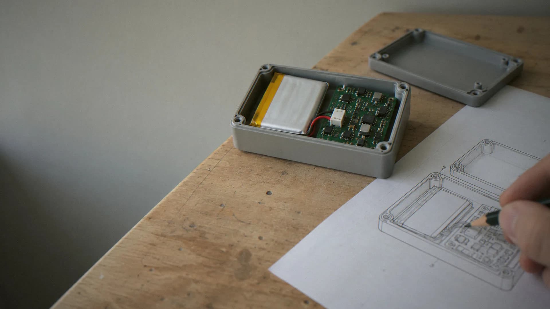
What does electronics and mechanical product design include?
It covers the system architecture, the schematic, the PCB layout and the enclosure with its mechanical parts. One team draws all four, so the board fits the housing and the housing can be molded. You receive schematics, layout files, Gerbers, a BOM and enclosure CAD, with a written report at each stage gate.
What we design
When the board and the enclosure come from two firms, the gap between them becomes your problem. A connector misses its opening. A battery has no room to swell. An antenna ends up boxed in by a metal frame. Each firm can show that its own part is right, and the product still does not work. One team removes that gap, because the same engineers own both sides of the interface.
The same logic covers firmware. The schematic sets which pins, buses and power rails the firmware can use, so our firmware engineers review the schematic before layout starts.
- System architecture. The block diagram, the power budget, the choice of microcontroller or module, and the radios. We check parts availability and alternates here, before the schematic is drawn.
- Schematic. The circuit, with simulation at the depth the product needs and a second-engineer check before delivery.
- PCB layout. Placement and routing, the stack-up, controlled impedance where it matters, and the Gerbers and files the Shenzhen factory fabricates the board from.
- Enclosure and mechanical parts. The housing, internal frames, buttons, light pipes, seals and the parts that hold the board.
- Stage-gate sign-off. A review with you at the end of each step, before the next one starts.
How a design moves through the stage gates
- Requirements. You describe what the product must do, its size, its power source, the budget and the date. We return a written specification, a block diagram and a first enclosure envelope.
- Schematic. We draw and simulate the circuit and pick parts with a supply you can buy. You receive the schematic source, a PDF and the first BOM.
- Layout. Placement comes first, then routing. You can approve placement before routing starts. You receive the layout source, Gerbers, the BOM and the placement file.
- Mechanical CAD. We finish the housing around the placed board. You receive native CAD, STEP files and drawings.
- Stage-gate sign-off. We review the design with you, hand over the files and move to the DFM review.
Board capability we design to
Every schematic and layout gets a second-engineer check before delivery. That engineer checks the power tree, the footprints, the connector pinouts and the parts against the BOM. A problem found there costs an edit, not a board spin.
Dense boards for wearables and radios can need HDI or rigid-flex. See HDI PCB and the high-speed PCB stack-up design guide for signal integrity.
| Feature | What we design to |
|---|---|
| Trace and space, standard process | 3 mil |
| Trace and space, HDI process | 2.5 mil |
| Trace and space, advanced process | 2 mil |
| Smallest BGA pitch for assembly | 0.25 mm |
| Smallest part placed | 01005 package (0.4 mm x 0.2 mm) |
| Layers in an online PCB layout order | 2 to 16 |
| EDA tools | The common layout tools, Altium and KiCad among them, or a conversion from yours |
Where do the antenna and the battery go?
They are placed first, with the enclosure, because both are hard to move later. The antenna needs a keep-out zone free of copper, metal and the battery. The battery needs room to swell and a path for heat. We fix both positions in the first envelope, then route the board around them.
Radios fail quietly. A board can pass every bench test and still lose range once it sits in the housing, next to a hand or a metal frame. We check the antenna position against the enclosure model before layout, and again on the demo build in its real housing.
Do I need schematic design or only PCB layout?
You need only layout when the schematic is complete, reviewed and has footprints for every part. You need schematic design when you have a working idea, a dev-kit prototype or a partial circuit. If you are not sure, start with project initiation: an engineer checks feasibility, picks the major parts and estimates the BOM cost.
The online layout order starts from your finished schematic. Circuit design, simulation and copying an existing board sit outside it; we scope that work as schematic design or as an engineering project.
When does enclosure design start?
It starts with the requirements, not after the board is done. The enclosure sets the board outline, the connector positions, the battery space and where the antenna can sit. We draw a first envelope before layout, then finish the housing around the placed board so both reach the DFM review together.
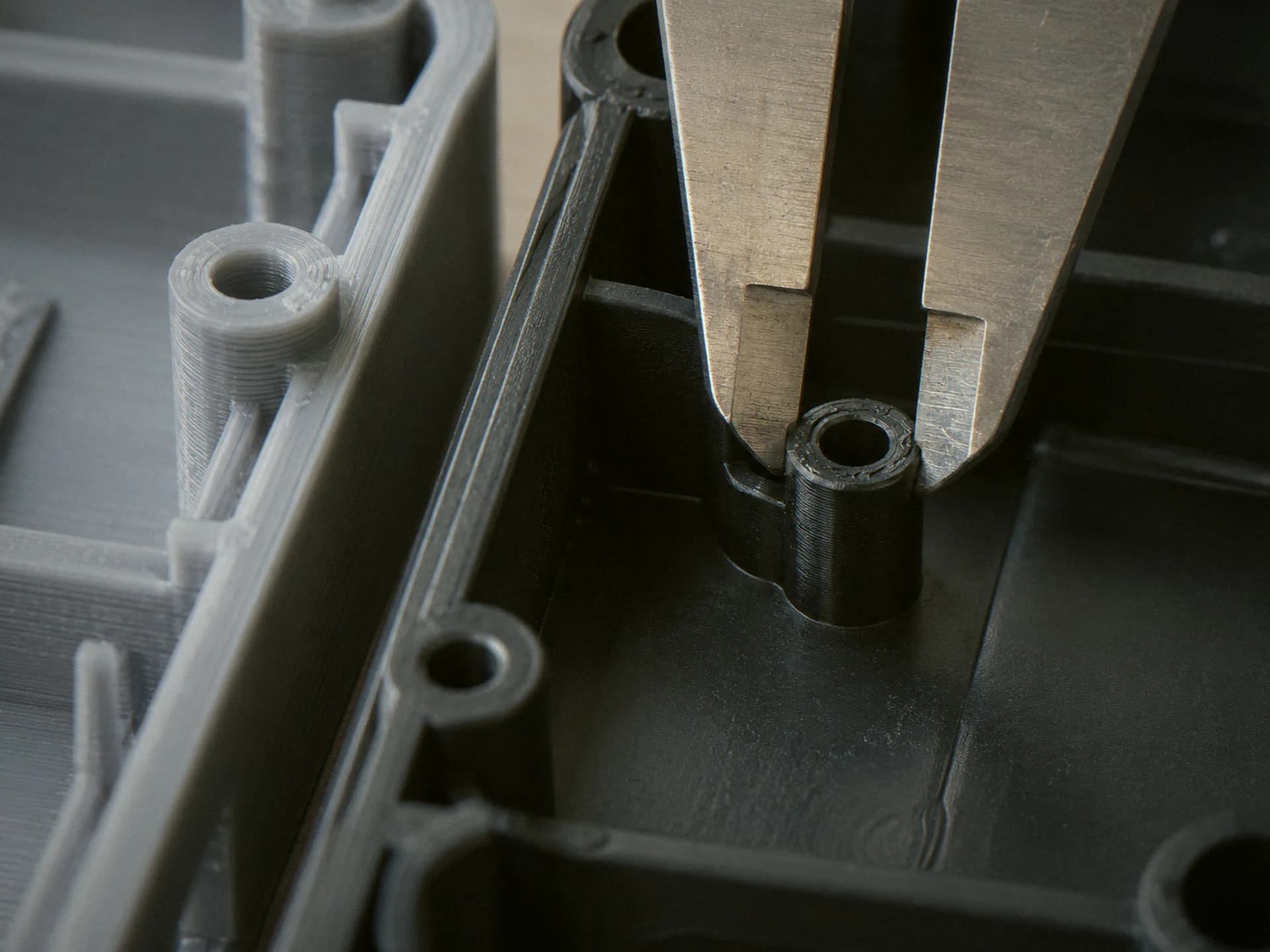
For a demo build, the housing can be printed or machined. For production it is molded, and molding sets rules for draft, wall thickness and ribs. We design to those rules from the first envelope, so the demo build housing does not need a redesign before tooling. See injection molding for the production side.
Which design files do I own?
On an engineering project, all of them. You receive the design source files at each stage gate: schematic and layout source, Gerbers, the BOM, native enclosure CAD and STEP files. On a fixed-scope portal order, the scope you approve states the output format and who owns the files.
Order design work online
The three design services get a free engineering review in 2 business days. A full product design with enclosure and firmware is scoped with an engineer and priced in an official quote.
- Project initiation: feasibility, the major parts and a BOM cost estimate, at a published fixed price.
- Schematic design: priced in tiers by the number of parts and modules, with simulation and review.
- PCB layout: a new layout or a controlled change, with optional approvals of placement and routing.
- Custom mechatronic parts & assemblies: mechanisms, housings and tested subassemblies. Price from a specialist within 24 hours on business days.
Recent work: light leaking where the display met the shell
A smart home company had its housing, its HDI board and its display from separate vendors, and light leaked where the display met the overmolded shell. In the Shenzhen factory, the assembled board went into the housing mold as an insert, and the light guide was molded into the housing. That removed a separate display part. Read the case study.
Facts and questions
Can you start from a dev-kit prototype?
Yes. A dev-kit build with jumper wires is a good start: it shows which parts work together. We turn it into a schematic, choose parts that can be bought in volume, and design a board and a housing around them. Firmware written for the dev kit can move across with modest changes.
Can you design for a regulated product?
Yes. We design to the documentation the Shenzhen factory's ISO 13485, IATF 16949 and AS9100 systems require. The FDA path runs with your regulatory team.
Can you design flex or rigid-flex boards?
Yes. Wearables, smart glasses and data gloves need a board that bends or folds into a small housing. We design the stack-up, the bend zones and the stiffeners with the enclosure, then check them in the DFM review. See flex PCB and rigid-flex PCB for the build side.
The Shenzhen factory fabricates rigid-flex boards up to 40 layers through engineering review.
How is design work priced?
Project initiation, schematic design and PCB layout show a published fixed price in the portal. A full product design is scoped by an engineer after a free engineering review and priced in an official quote. Nothing is charged when you submit, and you see the findings before you accept.
Tell us what you are building
- An engineer runs a free engineering review of your files, and nothing is charged when you submit.
- You see the findings first.
- We publish the official quote with an itemized total, lead time and validity window.
- You accept the official quote, and only then does payment open.