HDI PCB: microvias, via-in-pad and sequential lamination
A fine-pitch BGA usually decides whether your board needs HDI. Our engineers plan the via structure and the stack-up while the schematic is still open.
No CAD yet? Our design team can take it from a sketch or a spec.
Walk Shenzhen factories with us, Dec 6–11. See the tour
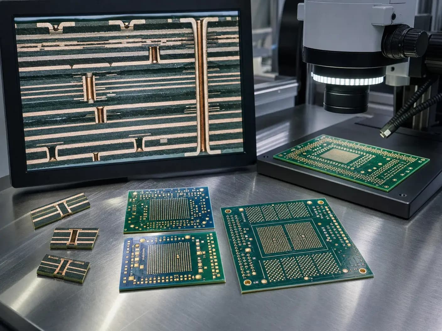
An HDI board has more interconnect density than drilled through-holes can give. Laser-drilled microvias join one layer to the next, and each level is built in its own lamination cycle. The reason is almost always a package: a BGA whose pitch leaves no room to route a signal out between through-holes. Illuminious is a U.S. NPI engineering company. Engineered in San Francisco. Prototype builds, DFM and mass production in our own factory in Shenzhen. HDI is configured in the Advanced PCB & PCBA route, and every via type except a plain through-hole goes to engineering review, because the yield of a microvia structure depends on the whole stack-up.
Design the escape routing before you design the board
Each build-up level adds one more pass through press, drill, plate and inspect, so the cheapest HDI decision is often the one that removes a level. Most HDI cost is fixed in the design phase. The package choice sets the pitch. The pitch sets the via size and the number of build-up levels. The levels set the lamination cycles, and each cycle is a new chance for layer-to-layer registration to drift. When our engineers draw the schematic, they check parts availability and alternates first, and they ask whether a package with a coarser pitch does the same job. A second engineer then checks the schematic and the layout (power tree, footprints, connector pinouts, parts against the BOM) before delivery.
Via-in-pad needs the same early care. A via inside a BGA pad must be filled and capped, or solder drains down the barrel during reflow. Via-in-pad does not by itself need the advanced route: the standard route asks for the via plating method, and "Filled and plated over" goes to engineering review there. Our DFM review in the design phase sorts each finding by when it must be fixed: before the demo build, before EVT, or before production. Signal integrity is the other reason for HDI. Short microvias leave short stubs and low parasitic inductance, which helps fast digital links. Controlled impedance is declared with its targets and the critical nets named, held to ±5% impedance and checked by TDR testing. Low-loss and Rogers laminates are declared laminate families. Boards above the configurator's 30 layers, up to 40 layers, are quoted after engineering review.
Order HDI boards online
Configure the board in the Advanced PCB & PCBA route, upload your files privately, and submit it. An engineer reviews it within 24 hours on business days, and the official quote follows. Configure an HDI board
HDI capabilities
| Capability | What it covers |
|---|---|
| Fine-line routing | Trace and space of 2.5 mil on the HDI process. Below the configurator's 0.10 mm minimum, down to 2 mil (0.05 mm), through engineering review. |
| Laser-drilled microvias | A declared smallest via diameter from 0.05 to 0.5 mm. A microvia joins one layer to the next, which frees the space under a dense package. |
| Stacked and staggered structures | Both are declared via options and both go to review. Up to 14 stacked microvia layers. The escape routing decides which structure the board needs. |
| Via-in-pad | Filled and plated-over vias, so a via can sit inside a BGA pad. On the standard route this is a review field. |
| Sequential lamination | Up to 4 sequential-lamination cycles (4+N+4). Declared per project, so the review plans the build cycles before fabrication starts. |
| Controlled impedance | ±5% impedance with TDR testing, declared with impedance targets and the critical nets named. |
| Rigid-flex HDI | Rigid-flex is a declared board class in the advanced route. See rigid-flex PCB. |
| Assembly of fine-pitch parts | Placement down to 0.25 mm BGA pitch on 8 automated SMT lines in the Shenzhen factory, with X-ray inspection as a declared option on this route. |
How an HDI board moves from layout to assembly
| Step | What we do | What you get or decide |
|---|---|---|
| 1. Stack-up and via plan | Our engineers read the package pitches and plan the via structure, the build-up levels and the laminate. | You approve the stack-up before layout is locked. |
| 2. Engineering review | An engineer checks the fabrication package against your declared configuration: drill structure, feature sizes, panel and yield risks. | You see the findings and the official quote before you pay. |
| 3. Inner layers and lamination | We image and inspect the core layers, then laminate, laser-drill, plate and fill each build-up level. | The sequential lamination plan you approved, run in that order. |
| 4. Outer layers and finish | We image and etch the outer layers, then apply solder mask and the declared surface finish. | You choose the finish and the inspection level in the order. |
| 5. Test and assembly | We test the boards electrically and check impedance by TDR. The Shenzhen factory assembles them and inspects hidden joints by X-ray when declared. | Boards with test records, built to IPC-6012 Class 3 where you specify it. |
What HDI gives a product
Smaller boards
Finer lines, microvias and via-in-pad put more routing in less area. That matters most in wearables such as smart rings and smart glasses, where every square millimeter goes to the battery.
Cleaner fast signals
Short microvias leave short stubs and low parasitic inductance and capacitance, so high-speed links lose less signal.
Room for fine-pitch packages
Via-in-pad lets a high-pin-count BGA or CSP escape on inner layers, with the via filled so solder stays in the joint.
Fewer layers, sometimes
A well-planned HDI stack can replace a thick through-hole board. The review tells you whether that trade saves money on your design.
How do I know whether my design needs HDI?
Start from the densest package on the board. If its pitch leaves no room to route a signal between two vias at your minimum trace and space, you are at the HDI boundary. If the board is only small or only crowded, better placement and more layers usually solve it without HDI.
A second test is the layer count. If through-hole routing pushes the stack past what the board can carry mechanically, microvias may bring it back. Trace and space below the configurator's 0.10 mm minimum, down to 2 mil (0.05 mm), is quoted after engineering review, and so are boards above 30 layers. If you are not sure, send the BGA part numbers with the order; our engineers answer this question in the free engineering review.
What is the difference between stacked and staggered microvias?
Staggered microvias are offset from one level to the next, so no via sits on another. Stacked microvias sit on top of each other and route straight down, which uses less area. Stacked is denser and harder to build, because each level must be filled flat enough for the next one to land on it.
A defect at any level of a stacked column can fail the whole column, so a staggered structure is the more forgiving build when the routing allows it. Both are declared options and both go to engineering review. The choice follows from the escape routing.
Why does HDI need more than one lamination cycle?
A laser can only drill a microvia through the outer dielectric layer that is being formed. To reach deeper, the board is laminated, drilled, plated and filled, then laminated again with the next layer pair. Each cycle repeats press, drill, plate and inspect, and each one adds cost and registration risk.
This is the real cost of HDI, and the number of build-up levels is a design decision worth time. We run up to 4 sequential-lamination cycles. Sequential lamination, backdrill and press-fit holes are each declared per project, so the review plans the process around them early. A high-speed stack-up guide explains how layer order affects the same decision.
Advanced-route interconnect options in the configurator
These are the limits the advanced board configurator accepts; a board outside them goes to an engineer.
Declared optionSettings available
- Board class
- HDI, RF / high frequency, Power / heavy copper, High layer count, Rigid-flex
- Via technology
- Through via, Blind / buried, Laser microvia, Stacked microvia (all except through via go to review)
- Smallest via diameter
- 0.05–0.5 mm
- Layer count
- 4, 6, 8, 10, 12, 14, 16, 18, 20, 24 or 30
- Laminate family
- High-Tg FR-4, Low-loss, Rogers / equivalent RF, Polyimide
- Maximum copper weight
- 1, 2, 3, 4 or 6 oz
- Sequential lamination
- Declared per project
- Backdrill
- Declared per project
- Press-fit holes
- Declared per project
- Controlled impedance
- Declared, with impedance targets and critical nets named
- Placements per board
- 0–10,000 when assembly is included
- Inspection
- Standard AOI, AOI + X-ray, or Advanced report and X-ray
- Review target
- Within 24 hours on business days after you submit
Recent work
A smart home startup needed a multilayer HDI board inside an overmolded enclosure, assembled into a finished product. Read the smart home HDI and box build case.
Facts and questions
What is a microvia?
A microvia is a laser-drilled via that joins one layer to the next layer instead of passing through the whole board. The advanced route accepts a declared smallest via diameter from 0.05 to 0.5 mm. Each microvia level is formed in its own lamination cycle, so the number of levels and the number of cycles are one decision.
Is via-in-pad the same thing as HDI?
No, but the two are close. Via-in-pad means a via sits inside a component pad, so it must be filled and capped or solder drains down the barrel. On the standard route, "Filled and plated over" is a via plating option that goes to engineering review. Microvias are what move a board to the advanced route.
Does an HDI board need X-ray inspection?
Yes, when it is assembled with the packages that made it HDI. Joints under a BGA or QFN cannot be seen by optical inspection. On the advanced route, inspection has three settings: standard AOI, AOI with X-ray, and an advanced report with X-ray. Choose X-ray for any board with bottom-terminated packages.
What is backdrilling, and when do I need it?
Backdrilling removes the unused part of a plated through-hole: the stub below the layer where the signal leaves. At high frequency that stub acts as a resonant antenna. Declare backdrill when the board carries multi-gigabit links. Below that speed, the stub rarely matters enough to pay for the extra operation.
What does the review check on an HDI stack-up?
Stack-up completeness and laminate availability, the via structure against the package pitches, microvia and lamination feasibility, copper balance, registration risk and the impedance approach. It also checks backdrill and press-fit holes where you declared them. Any change reaches you as an itemized revision before fabrication.
How your official quote is prepared
Configuring HDI fabrication in the Advanced PCB & PCBA route returns a live supplier price when suppliers can price the build. Otherwise a specialist prepares your official quote within 24 hours on business days. An engineer reviews every order. The review is free and comes before payment, and the official quote is the amount you pay.
Bring us the BGA before you bring us the board
Send the package list, a draft stack-up or a full layout. Our engineers plan the vias, review the files and publish the official quote before anything is charged. See also flex PCB and PCB assembly.
- An engineer runs a free engineering review of your files, and nothing is charged when you submit.
- You see the findings first.
- We publish the official quote with an itemized total, lead time and validity window.
- You accept the official quote, and only then does payment open.