Signal integrity in high-speed PCB design begins and ends with stackup architecture. As data rates push past 32 Gbps with PCIe 6.0, DDR5-6400, and USB4 Gen 4, the margin for stackup errors has collapsed to zero. A poorly designed stackup doesn't just degrade signal quality—it causes bit errors, EMI failures, and multimillion-dollar respins. This guide covers the critical stackup design principles that separate first-pass silicon from costly redesigns.
Why Stackup Design Determines Signal Integrity
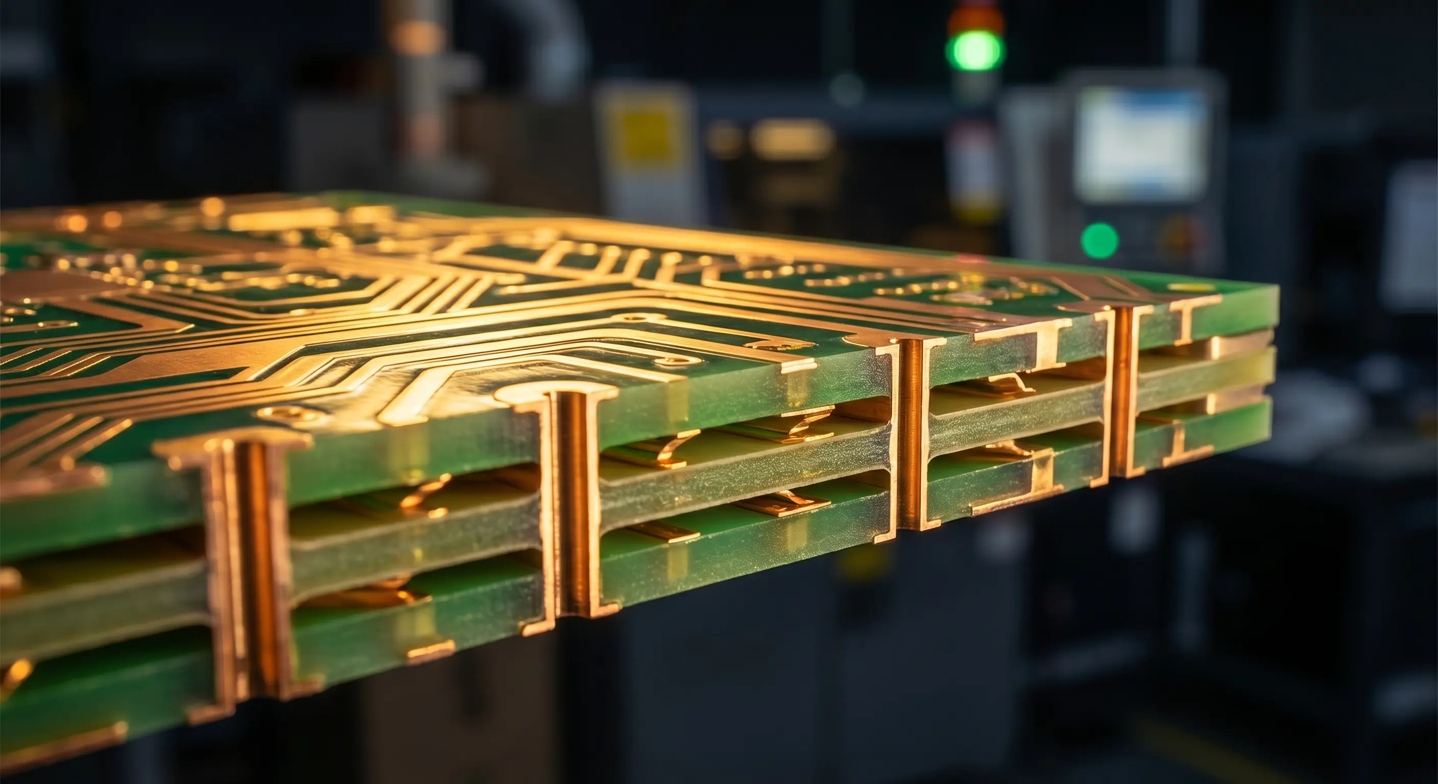
A PCB stackup is the vertical arrangement of copper signal layers, power planes, and dielectric material that forms your circuit board's cross-section. For high-speed designs, this vertical structure controls three fundamental signal integrity parameters: characteristic impedance, crosstalk coupling, and electromagnetic radiation.
Every signal trace on your board forms a transmission line with its reference plane. The distance between the trace and its reference, the dielectric constant of the material between them, and the trace geometry together determine the impedance. Get the stackup wrong, and no amount of routing cleverness will fix reflections, overshoot, or timing violations.
Impedance Control
Trace-to-reference distance sets impedance. A 1 mil variation in dielectric thickness can shift impedance by 2-3 ohms—enough to fail DDR5 or PCIe specs.
Crosstalk Suppression
Proper reference plane placement creates return path intimacy, reducing electromagnetic coupling between adjacent traces by 20-40 dB.
EMI Shielding
Continuous ground planes between signal layers act as Faraday shields, containing electromagnetic radiation and passing FCC/CISPR testing.
Power Delivery
Tight plane pairing creates embedded capacitance, reducing power distribution network impedance at frequencies above 100 MHz.
The Six Rules of High-Speed Stackup Design
Rule 1: Every Signal Layer Needs an Adjacent Reference Plane
This is the single most important stackup rule. Every signal layer must have a solid, continuous reference plane (ground or power) on at least one adjacent layer—ideally within 3-5 mils. When a signal transitions between layers through a via, its return current must also transition. If the reference planes aren't connected nearby, the return current finds a long, winding path, creating a loop antenna that radiates EMI and degrades signal quality.
The Return Path Disaster
A 3 GHz signal on a 6-layer board with no adjacent ground plane showed 15 dB worse crosstalk and failed radiated emissions testing by 8 dB. Adding a ground plane directly adjacent to the signal layer fixed both issues simultaneously.
Rule 2: Route High-Speed Signals on Stripline Layers
Stripline traces—sandwiched between two reference planes—offer superior signal integrity compared to microstrip traces on outer layers. Stripline provides natural shielding from both sides, reducing crosstalk by 15-20 dB and emissions by 10-15 dB. Reserve outer layers for components, connectors, and low-speed signals.
- Microstrip (outer layer): Higher loss, more EMI, impedance varies with solder mask and environmental factors
- Stripline (inner layer): Lower loss, inherent shielding, stable impedance, preferred for signals above 1 GHz
- Broadside-coupled stripline: Best for differential pairs—tight coupling in Z-axis provides superior mode conversion performance
Rule 3: Use Symmetric Stackup Structures
A balanced stackup—where the layer arrangement is symmetric about the board's centerline—prevents board warpage during manufacturing. Warped boards cause assembly defects, connector misalignment, and thermal reliability failures. For a 6-layer board, this means matching Layer 1 with Layer 6, Layer 2 with Layer 5, and Layer 3 with Layer 4 in both copper weight and dielectric thickness.
Rule 4: Pair Power and Ground Planes Tightly
Power-ground plane pairs with thin dielectric (2-4 mils) create embedded planar capacitance. This distributed capacitance provides low-impedance power delivery at high frequencies where discrete decoupling capacitors become inductive. For DDR5 and PCIe designs, this embedded capacitance is essential for maintaining clean power rails above 1 GHz.
Plane Spacing vs. Capacitance
2 mil spacing: ~500 pF/in²
4 mil spacing: ~250 pF/in²
10 mil spacing: ~100 pF/in²
Tighter spacing = better high-frequency decoupling
Material Matters
High-Dk prepreg between power-ground pairs increases embedded capacitance by 3-4x. Materials like 3M C-Ply or DuPont Interra provide Dk values of 20-40 specifically for embedded capacitance layers.
Rule 5: Manage Via Transitions for Layer Changes
When high-speed signals change layers through vias, the return current must follow. Without nearby stitching vias connecting the reference planes, the return current discontinuity creates impedance reflections and EMI. Place ground stitching vias within 50 mils of every signal via for high-speed nets. For differential pairs, place stitching vias symmetrically to maintain mode balance.
Rule 6: Choose Dielectric Materials for Loss Budget
Standard FR-4 (Df ≈ 0.02) works fine for signals below 3 GHz. Above that, dielectric loss dominates and signal attenuation becomes unacceptable. Material selection directly impacts the channel loss budget:
Standard FR-4
Dk: 4.2-4.5
Df: 0.015-0.020
Best for: Signals below 3 GHz, cost-sensitive designs
Loss at 10 GHz: ~1.2 dB/in
Mid-Loss Materials
Examples: Megtron 6, IS410
Dk: 3.5-4.0, Df: 0.006-0.010
Best for: DDR5, PCIe 3.0-4.0, 10GbE
Loss at 10 GHz: ~0.7 dB/in
Low-Loss Materials
Examples: Megtron 7, RO4350B
Dk: 3.0-3.5, Df: 0.003-0.006
Best for: PCIe 5.0-6.0, USB4, 112G SerDes
Loss at 10 GHz: ~0.4 dB/in
Ultra-Low-Loss
Examples: Megtron 7N, IT-968G
Dk: 3.0-3.3, Df: 0.001-0.003
Best for: 224G SerDes, 800G Ethernet
Loss at 10 GHz: ~0.25 dB/in
Reference Stackup Configurations
6-Layer Stackup for DDR5 and PCIe 3.0
The 6-layer stackup is the workhorse for embedded computing, networking, and consumer electronics. It balances cost and performance for designs running up to 8 GT/s.
Layer 1 — Top Signal (Microstrip)
Component side, low-speed signals, impedance-controlled microstrip for short high-speed runs.
Layer 2 — Ground Plane
Continuous ground reference for Layer 1. Critical for impedance control and EMI shielding.
Layer 3 — Inner Signal (Stripline)
Primary high-speed routing layer. DDR5 data lines, PCIe traces, USB3 signals. Sandwiched between L2 GND and L4 power.
Layer 4 — Power Plane
Split power planes for VDDQ, VTT, core voltage. Tight coupling to L5 ground creates embedded capacitance.
Layer 5 — Ground Plane
Second ground plane. Provides reference for L6 signals and forms plane pair with L4.
Layer 6 — Bottom Signal (Microstrip)
Secondary component side. Route non-critical signals and escape routes.
8-Layer Stackup for PCIe 5.0 and USB4
When data rates exceed 16 GT/s, you need dedicated signal-reference pairs and better isolation. The 8-layer stackup provides four signal layers with independent reference planes.
Signal + Ground: Top microstrip with adjacent ground. Fine-pitch BGA escape routing.
Stripline Signal + Power: Primary high-speed routing between ground (L2) and power (L4). Dual-reference stripline for best impedance stability.
Power + Stripline Signal: Power plane references L6 signals. Route second set of high-speed lanes here.
Ground + Signal: Bottom microstrip with adjacent ground. Symmetric to L1/L2.
10-Layer Stackup for PCIe 6.0 and 112G SerDes
At 32 GT/s and beyond, every fraction of a dB matters. The 10-layer stackup adds dedicated power-ground pairs and provides the signal isolation needed for cutting-edge protocols.
Key Advantage: Dual Stripline Pairs
The 10-layer stackup provides two independent stripline signal layers (L3 and L8), each sandwiched between a ground and power plane. This allows routing the most sensitive signals—112G SerDes, PCIe 6.0 lanes—with minimal crosstalk from other nets. The additional power-ground pair also provides superior PDN impedance.
Impedance Control: The Math That Matters
Controlled impedance isn't optional for high-speed design—it's a hard requirement. DDR5 specifies 40Ω single-ended with ±7% tolerance. PCIe 6.0 requires 85Ω differential with ±10% tolerance. USB4 demands 85Ω differential with ±5% tolerance. Missing these targets causes reflections that degrade eye diagrams and increase bit error rates.
Trace Width
Wider traces = lower impedance. For 50Ω on FR-4 with 4 mil dielectric, trace width is approximately 6-7 mils.
Dielectric Thickness
Thinner dielectric = lower impedance. This is why tight coupling to reference planes is so powerful.
Dielectric Constant
Higher Dk = lower impedance. Material choice directly sets the trace geometry required for target impedance.
Copper Thickness
Thicker copper = lower impedance. 1 oz copper shifts impedance down ~2Ω vs. half-oz for the same trace width.
Best practice: Specify impedance requirements directly on your fabrication drawing. Let your fab house calculate exact trace widths based on their specific material lots and press stack. Request an impedance test coupon on every panel to verify compliance.
Crosstalk Mitigation Through Stackup Architecture
Crosstalk is the unwanted coupling of energy between adjacent traces. It comes in two flavors: near-end crosstalk (NEXT) and far-end crosstalk (FEXT). Both are directly controlled by stackup geometry.
- Reduce trace-to-reference distance: Halving the distance to the reference plane reduces crosstalk by approximately 6 dB. This is the most effective single action you can take.
- Orthogonal routing on adjacent layers: Route signals on Layer 3 horizontally and Layer 5 vertically. This eliminates broadside coupling between layers.
- Guard traces with ground vias: For ultra-sensitive nets, add grounded guard traces spaced 3x the trace width from the victim net.
- Differential pair routing: Tight pair coupling (spacing ≤ trace width) makes differential pairs immune to common-mode crosstalk.
The difference between a working 32 Gbps link and a failing one is often 2 mils of dielectric thickness variation. Stackup precision is not a manufacturing detail—it's a design requirement.— High-Speed Digital Design Handbook, 2025
Common Stackup Mistakes That Kill Signal Integrity
No Adjacent Reference
Routing high-speed signals on a layer with no adjacent ground/power plane. This creates uncontrolled impedance and massive return path loops.
Split Planes Under Traces
A signal crossing a split in its reference plane experiences a impedance discontinuity. Each crossing adds reflections and EMI.
Asymmetric Builds
Unbalanced copper distribution warps boards. Warped boards fail assembly, especially with fine-pitch BGAs and 0201 components.
Ignoring Fiber Weave Effect
FR-4 is woven glass and resin. Signals routed along glass fibers see a different Dk than signals between fibers. At 10+ GHz, this causes timing skew in differential pairs.
Working With Your Fabrication Partner
Your PCB fabricator is a critical partner in stackup design. They know the exact properties of their materials, the capabilities of their presses, and the tolerances they can achieve. Here's how to collaborate effectively:
- Share your impedance requirements early: Provide target impedance, tolerance, and protocol specs before layout begins.
- Request a stackup proposal: Let the fab house recommend the exact dielectric thicknesses and trace widths.
- Specify impedance test coupons: Every panel should include test coupons for verification.
- Discuss material alternatives: Your fab house may have cost-effective mid-loss materials not widely advertised.
- Review the stackup drawing: Cross-check the fab's proposed stackup against your impedance and loss budget calculations.
Illuminious Stackup Design Review Process
At Illuminious, we've optimized hundreds of high-speed PCB stackups for products ranging from AI accelerator cards to 5G base stations. Our stackup review covers:
Full-wave simulation of critical nets to verify impedance, loss, and crosstalk meet protocol specifications.
Cost-performance analysis to identify the optimal dielectric material for your signal speed and loss budget.
Manufacturability check ensuring the proposed stackup is producible with acceptable yields at your target volume.
Power delivery simulation verifying target impedance from DC to the highest harmonic frequency.
Stackup Design Is a Team Sport
The most successful high-speed designs result from early collaboration between hardware engineers, SI specialists, and PCB fabricators. Start the stackup conversation before you route a single trace. Share your requirements, listen to your fab house's recommendations, and verify with simulation and measurement.
A well-designed stackup is the invisible foundation that makes everything else work. Get it right, and your high-speed signals will thank you with clean eye diagrams, zero retries, and a product that works the first time.
Need expert stackup review for your next high-speed design? Contact Illuminious for comprehensive signal integrity analysis and stackup optimization.