AI servers are pushing PCB thermal management to its breaking point. With NVIDIA's latest accelerators drawing 1000W per chip and global data center investments projected to reach $7 trillion by 2030, the PCB beneath these power-hungry processors has become a critical thermal bottleneck. Traditional FR-4 designs simply cannot handle the heat flux densities of modern AI workloads. This guide covers the advanced thermal management strategies that hardware engineers and PCB designers need to keep next-generation AI servers running within safe operating temperatures.
The Thermal Crisis in AI Server PCBs
AI servers generate heat densities that were unimaginable five years ago. A single NVIDIA H100 GPU draws 700W, while the Blackwell architecture pushes past 1000W. When you pack 8 of these accelerators onto a single server board, the PCB must manage and route heat from components dissipating over 5kW collectively—all while maintaining signal integrity at 32 Gbps and beyond.
The challenge is multidimensional. Heat doesn't just flow upward through heatsinks. It conducts laterally through copper planes, downward through thermal vias into internal layers, and radiates across the board surface. Without deliberate thermal design at the PCB level, hot spots form under BGA packages, causing solder joint fatigue, via cracking from CTE mismatch, and accelerated electromigration in traces.
Junction Temperature
AI accelerator junction temps must stay below 85-95°C. Each 10°C rise halves component lifespan. PCB thermal resistance directly impacts the thermal ceiling.
Current Density
High-current power delivery traces (50-100A per rail) generate I²R heating. Thick copper and proper via arrays are non-negotiable for power integrity.
CTE Mismatch
Different thermal expansion rates between copper, FR-4, and BGA solder balls cause mechanical stress during thermal cycling, leading to via and solder failures.
Warpage Control
Uneven heating across large PCBs (up to 18"×24" for AI servers) causes board warpage that disrupts BGA solder joint formation during reflow and operation.
Thermal Via Design Strategies
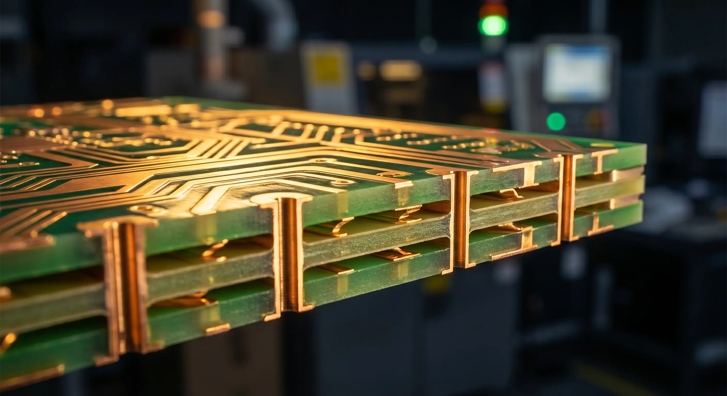
Thermal vias are the workhorse of PCB heat dissipation. These plated-through holes create vertical heat pipes that conduct thermal energy from component pads through the board to opposite-side heatsinks or thermal pads. For AI server PCBs, thermal via design requires precision engineering.
Via Array Design Parameters
The thermal resistance of a via array depends on three factors: via diameter, plating thickness, and array density. A standard 0.3mm via with 25μm copper plating has a thermal resistance of approximately 70-80°C/W per via. For a 1000W chip, you need a substantial via array to achieve acceptable thermal resistance.
Thermal Via Design Rules for AI Servers
Via diameter: 0.3-0.5mm (smaller vias allow higher density arrays)
Copper plating: ≥25μm (1 oz) for adequate thermal conduction
Array pitch: 0.8-1.2mm grid under BGA thermal pads
Via fill: Epoxy or copper-filled vias for maximum thermal transfer
Coverage: Target 30-50% via area coverage under high-power pads
Copper-filled vias offer 3-5x better thermal conductivity compared to standard plated-through holes. While more expensive, they're essential for AI accelerator boards where every degree of thermal margin counts. OKI's new AI server EMS production line, launched in March 2026, specifically features proprietary high heat dissipation technology built on advanced copper-filled via structures.
Via-in-Pad for BGA Thermal Management
For BGA packages with power-dissipating balls, via-in-pad construction is critical. Placing thermal vias directly in the BGA land pads minimizes the thermal resistance path from the chip junction to the PCB interior. The vias must be filled and planarized to prevent solder wicking during assembly.
- Active pad vias: Place under power and ground BGA balls carrying highest current
- Thermal land vias: Dedicated thermal pad areas with dense via arrays under exposed-die packages
- Copper coin vias: Solid copper inserts for extreme thermal loads, offering 10x the conductivity of plated vias
- Stitching vias: Perimeter vias around thermal zones that connect copper planes across all layers
Metal-Core PCB Technology for AI Servers
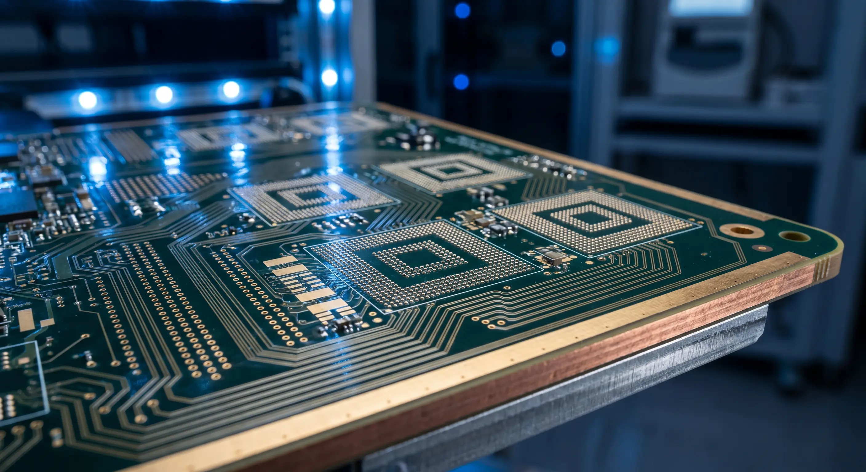
When FR-4's thermal conductivity (0.3-0.4 W/mK) can't handle the heat, metal-core PCBs (MCPCBs) enter the picture. MCPCBs replace the standard fiberglass core with an aluminum or copper baseplate, dramatically increasing lateral heat spreading.
Standard FR-4
Thermal conductivity: 0.3-0.4 W/mK
Best for: Low-power control logic
Max heat flux: ~5 W/cm²
Cost: Baseline
Aluminum Core PCB
Thermal conductivity: 1.0-2.0 W/mK (with dielectric)
Best for: LED lighting, mid-power boards
Max heat flux: ~15 W/cm²
Cost: 2-3x FR-4
Copper Core PCB
Thermal conductivity: 2.0-4.0 W/mK (with dielectric)
Best for: High-power RF, power electronics
Max heat flux: ~30 W/cm²
Cost: 5-8x FR-4
Embedded Copper Coin
Thermal conductivity: 385 W/mK (pure copper path)
Best for: AI accelerator hot spots
Max heat flux: ~50+ W/cm²
Cost: 8-12x FR-4
For AI server applications, the most effective approach combines a standard multilayer FR-4 stackup with embedded copper coins or heavy copper inserts under the hottest components. This hybrid approach maintains signal integrity on high-speed layers while providing dedicated thermal conduits through the board thickness.
Copper Thickness Optimization
Copper weight—measured in ounces per square foot—directly impacts both electrical performance and thermal management. Standard PCBs use 0.5 oz to 1 oz copper. AI server boards routinely specify 2 oz, 3 oz, or even heavier copper on power and ground layers.
1 oz Cu (35μm)
Standard for signal layers. Adequate for most routing but insufficient for high-current power delivery in AI servers.
2 oz Cu (70μm)
Minimum for AI server power planes. Handles 10-15A per 100mil trace. Reduces IR drop and I²R heating significantly.
3 oz Cu (105μm)
Preferred for AI server ground and power layers. Superior heat spreading across the board. Common for inner layers.
4+ oz Cu (140μm+)
Extreme power applications. Requires wider trace/space design rules. Used for busbar replacement on very high-current rails.
Design consideration: Heavy copper increases minimum trace/space requirements. While 1 oz copper supports 3/3 mil trace/space, 3 oz copper typically requires 8/8 mil minimum. This impacts BGA escape routing density. The solution: use heavy copper on internal power/ground layers while keeping 1 oz on signal layers for fine-pitch routing.
Advanced Stackup Thermal Design
AI server PCB stackups are engineering marvels—16 to 24 layers combining signal integrity, power delivery, and thermal management. Thermal design must be integrated into the stackup architecture from day one.
Step 1 — Thermal Mapping
Identify all high-power components and their dissipation values. Create a thermal map showing heat flux density across the board surface.
Step 2 — Copper Allocation
Assign heavy copper (2-3 oz) to power and ground layers. Dedicate copper flood fills on unused signal layer areas as thermal spreading planes.
Step 3 — Via Infrastructure
Design thermal via arrays under all high-power components. Connect thermal planes across layers with stitching vias on 2-3mm grid spacing.
Step 4 — Material Selection
Choose low-loss dielectrics for high-speed signal layers and high-thermal-conductivity prepreg for power-ground plane pairs. Macdermid Alpha's ALPHA HiTech CF31-4026, unveiled at IPC APEX EXPO 2025, represents the latest generation of high-temperature PCB materials engineered for exactly this application.
Step 5 — Simulation and Verification
Run coupled electrical-thermal simulations to verify junction temperatures, via temperatures, and board warpage under worst-case operating conditions before fabrication.
Liquid Cooling Interface PCB Design
Air cooling has reached its practical limit for AI servers. Liquid cooling is now mandatory for high-density AI compute racks, and PCB design must accommodate direct-to-chip liquid cooling hardware.
PCB Design Considerations for Liquid Cooling
- Cold plate mounting hardware: Design keep-out zones and mounting holes for cold plate brackets. These apply 20-50 lbs of clamping force that the PCB must withstand without flexing near BGA joints.
- Thermal interface material (TIM) wells: Recessed pad areas that contain TIM under the cold plate. Precise depth control prevents TIM pump-out during thermal cycling.
- Leak detection routing: Route leak sensor traces near liquid cooling connections. Condensation and leaks are the top reliability risk for liquid-cooled servers.
- Drip-proof conformal coating: Selective conformal coating around liquid cooling interfaces while leaving TIM contact areas bare.
- Manifold mounting features: Board edge features for liquid manifold attachment with strain relief for flexible tubing connections.
Google's 2026 patent filings reveal heterogeneous TIM architectures that place different thermal interface materials over different dies within the same package lid. This approach optimizes thermal transfer for multi-chip modules where power dissipation varies significantly across the package surface.
Thermal Simulation and Validation
Modern thermal simulation tools have become indispensable for AI server PCB design. Siemens reports that AI-driven design space exploration can automatically parameterize thermal variables—materials, floorplan geometry, microchannel dimensions, and TIM properties—and simulate hundreds of configurations to find optimal solutions.
Validation Checklist
Thermal simulation: CFD analysis with actual power maps, not worst-case uniform heating
IR thermal imaging: Validate simulation against physical prototypes under load
Thermal cycling tests: 1000+ cycles from -40°C to +125°C to verify via and solder reliability
Power cycling: Rapid power transients mimicking AI training workloads
Warpage measurement: Shadow moiré at reflow temperatures to verify coplanarity
Emerging Trends in PCB Thermal Management
The PCB thermal management landscape is evolving rapidly to keep pace with AI power demands:
Graphene Thermal Layers
Graphene-infused prepreg and copper-graphene hybrid foils promise 5-10x thermal conductivity improvement over pure copper. Expected in production PCBs by 2027-2028.
AI-Optimized Thermal Design
Machine learning algorithms that optimize via placement, copper allocation, and stackup configuration for thermal performance. Siemens and Diabatix are leading this approach.
Embedded Cooling Channels
Microfluidic channels embedded directly in the PCB substrate for direct liquid cooling of the board itself, not just the components mounted on it.
Smart Thermal Monitoring
On-board temperature sensors with real-time feedback to workload managers that throttle less-critical tasks to keep thermals in check during peak AI training runs.
Key Takeaways for PCB Designers
AI server PCB thermal management is no longer an afterthought—it's a first-class design constraint that must be addressed from the schematic stage. The boards that succeed combine multiple thermal strategies in a unified approach:
- Start thermal design early: Thermal constraints must influence component placement, stackup design, and layer allocation from day one
- Invest in thermal vias: Copper-filled via arrays under high-power components provide the most cost-effective thermal improvement
- Use heavy copper strategically: 2-3 oz copper on power and ground layers provides thermal spreading without sacrificing signal layer routing density
- Plan for liquid cooling: Even if your first generation uses air cooling, design the PCB to accommodate cold plate mounting in future revisions
- Simulate before fabricate: Coupled electrical-thermal simulation catches problems that cost 100x more to fix after prototyping
- Validate with real workloads: AI training creates thermal profiles different from steady-state testing. Test with actual inference and training loads
The convergence of rising AI power demands, massive data center investment, and advancing PCB manufacturing capabilities makes thermal management the defining engineering challenge for AI server hardware. Engineers who master these techniques will build the infrastructure powering the next decade of artificial intelligence.