Telecom and networking hardware: RF, speed and heat
Network hardware runs around the clock for years, in racks or on poles. Its boards mix high-speed digital lanes, radio signals and high power in a small space, so impedance, heat and part availability decide whether it works in the field. Our engineers design those boards and enclosures. Engineered in San Francisco. Prototype builds, DFM and mass production in our own factory in Shenzhen.
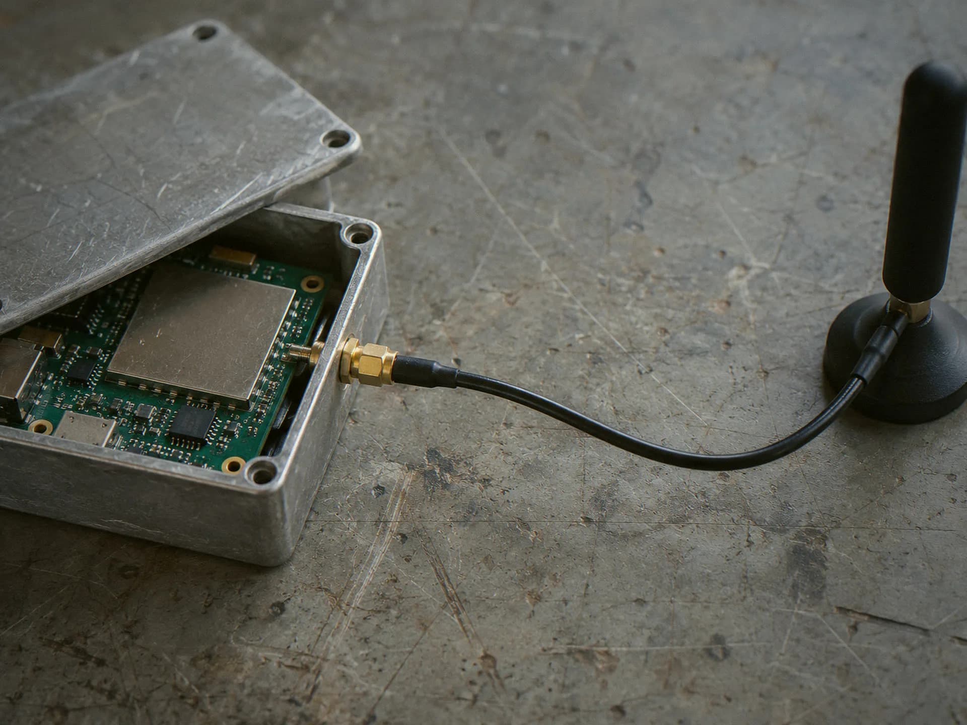
Why does signal integrity decide whether a network board works?
Because density works against it. Radio and high-speed lines need tight impedance through many layers, often on mixed RF and digital materials. Processors and power stages pack heat into a small space. The product must also stay buildable for years. These limits are set in the stackup and the layout, before the first board is fabricated.
Hardware in this field
The field covers radio units and small cells, optical modules and line cards, switches and routers, satellite and microwave backhaul, network security appliances, edge compute boxes and broadband equipment. Each mixes RF, high-speed digital and power on dense boards, which is the engineering we focus on.
What we engineer for telecom and networking
Controlled impedance and stackups. Hybrid stackups that put RF layers on low-loss laminates such as Rogers and digital layers on FR-4, with test coupons to confirm impedance. See HDI PCB.
Layer count and board size. The configurator takes up to 30 layers; through review, boards go to 40 layers and to 610 x 914 mm.
Heavy copper for power. Outer copper from 0.5 oz to 20 oz through review, for power stages and distribution.
Heat. Thermal simulation of processors and power stages, then heat sinks, vias and airflow tested on DVT units.
Outdoor housings. Sealed enclosures for heat, humidity and weather, designed with the antenna and the cable entries in mind. See sheet metal fabrication.
Integration and test. System assembly, firmware flashing and configuration testing, so units arrive ready to deploy. See box build.
Test access. High-speed lanes and RF paths are hard to probe once the board is built. Our engineers place test points and coupons in the layout, and the ICT and FCT stations run the production test firmware at PVT, so each unit is checked before it is packed.
How do you protect RF performance in a dense design?
By planning it in the layout. Our engineers route RF and high-speed lanes on controlled-impedance traces, keep digital noise off them with ground planes and stitching vias, and place shields and test points early. EMC and RF pre-scans run on DVT units, before formal certification, when a change still costs little.
Parts that stay available
Network hardware stays in service far longer than its parts stay in catalogs. Our engineers check availability and alternates before the schematic is drawn, and the sourcing team watches lifecycle notices across a network of 350 audited suppliers, so you hear about a last-time buy early.
Firmware and configuration
Network devices ship with bootloaders, board support and a configuration image loaded at the end of the line. Our engineers write and test that firmware on the demo build, keep firmware test results per serial number and ship production units with debug ports locked. See firmware development.
From idea to the first network board
If the product is at the idea stage, project initiation checks feasibility and picks the major parts, including the laminates and the processor. If you need the board drawn, see product design. If you have released files, order prototype boards in the portal after a free engineering review, and production runs from the same files once the design is validated. See quality and certifications for the Shenzhen factory's certificates.
Certification path
Carrier and central-office tests, such as NEBS, and radio approvals like FCC and CE are a certification path for your product. We plan design margin from the first layout, build DVT units for the lab and supply the documents it asks for. Your team or your lab files the submission.
Recent work: impedance on a hybrid RF stackup
A telecom hardware company needed tighter impedance control on mmWave antenna boards built on a hybrid stackup of RF and digital laminates. We changed the drill stack and lamination cycle, added impedance coupons to every panel and tested the RF traces on each one. Read the case study.
Questions about telecom hardware
Can you build prototypes of a dense RF board?
Yes. Advanced PCB & PCBA in the portal covers HDI, RF laminates and higher layer counts, at a live price before you submit. Boards beyond the configurator range go through review and an official quote.
Do you design the board, or only build it?
Both. Our engineers can draw the schematic, lay out the stackup and route the board, or take your released files and run a DFM review before the first build.
Do you certify for NEBS?
No. NEBS testing is done by accredited labs on your product. We design and build the units to the test plan and help prepare them for the lab. Design margin for heat, fire spread and electrical safety is planned from the first layout, because NEBS failures found late can mean a new board.
Tell us what you are building
- An engineer runs a free engineering review of your files, and nothing is charged when you submit.
- You see the findings first.
- We publish the official quote with an itemized total, lead time and validity window.
- You accept the official quote, and only then does payment open.