Flex PCB design and assembly
A flex circuit fails at the bend. Our engineers design the bend first: where it is, how tight it is, and whether it moves in service.
No CAD yet? Our design team can take it from a sketch or a spec.
Walk Shenzhen factories with us, Dec 6–11. See the tour
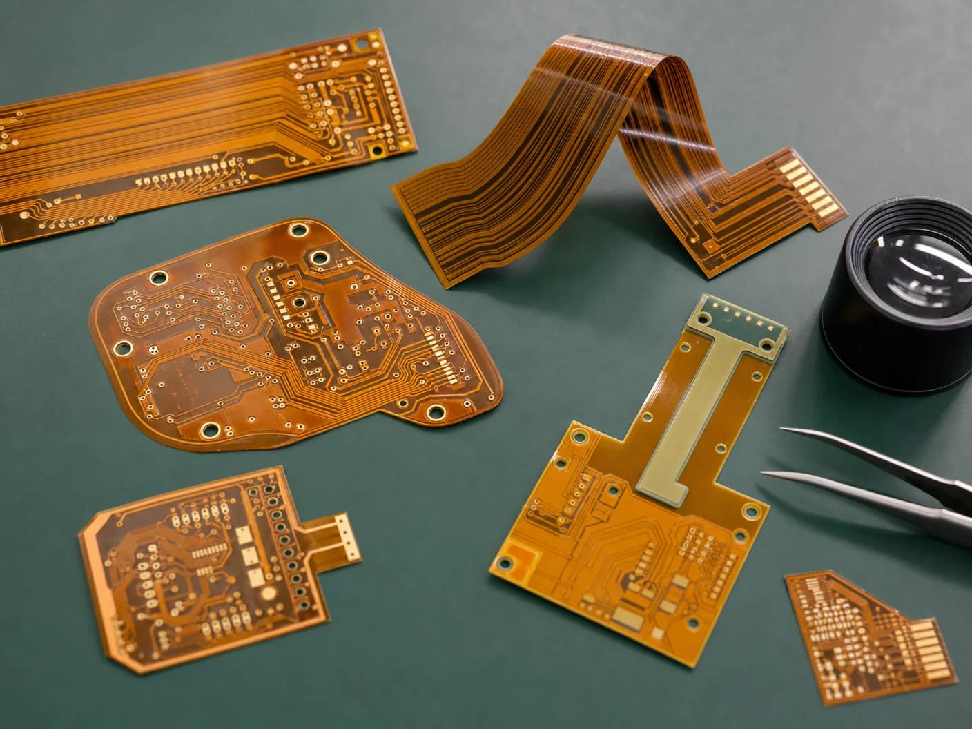
A flex PCB is a printed circuit built on thin polyimide film instead of glass-reinforced epoxy, so the finished circuit bends. That gives you one of two things. The circuit can replace a wire harness and its connectors by folding into a shape the product already has. Illuminious is a U.S. NPI engineering company. Engineered in San Francisco. Prototype builds, DFM and mass production in our own factory in Shenzhen. Or it can be a moving part that flexes again and again in service: a hinge, a print head, a folding display. Those two cases have almost nothing in common mechanically, and the design must choose between them first.
What a flex PCB is, and how it is ordered
Flexible circuits are configured through the advanced board route, because polyimide construction needs process planning. Single- and double-layer flex is quoted through engineering review; the advanced route's layer field starts at 4. Almost everything that makes a flex circuit hard is mechanical, and almost none of it shows in the Gerbers, so an engineer reads your drawing against the configuration you declare. If you have only a sketch of where the circuit must go, our engineers can draw the flex outline and the stack-up with you, through schematic design and PCB layout, before any board is ordered.
Design the bend first
Our engineers start with the product. They look at how the circuit sits in the enclosure, where it folds, and what moves. For a wearable, the flex often runs around a battery or along a strap. For a smart ring, it may wrap inside the shell. For a robot hand, it may cross a joint that moves all day. For a data glove used to train robots, it may run along each finger and flex with every grip. Each of these is a different bend, and each needs a different stack-up. Our engineers model the fold in the enclosure CAD, so the flex outline, the bend line and the parts around it are fixed together.
Next comes the stack-up. Layer count, copper type, grain direction and trace position relative to the neutral bend axis decide how long a moving circuit lasts. The DFM review checks bend radius, trace routing near the bend, coverlay openings, stiffener areas and the parts placed near the fold. Each finding is sorted by when it must be fixed: before the demo build, before EVT, or before production.
Then the circuit is built in the Shenzhen factory, to IPC-6013 Class 2 or Class 3, and assembled on its SMT lines. Boards get automated optical inspection, and firmware test results are kept per unit, by serial number, when the order includes functional test. The demo build tells you whether the fold works in your hand. EVT and DVT then prove it over many cycles before the design is closed, and the DFM review is repeated before DVT so a late change to the bend is caught while it is still cheap to fix.
Flex capabilities
| Capability | What it covers |
|---|---|
| Single- and double-layer flex | Polyimide circuits for static and dynamic use, quoted through engineering review. The bend radius your design needs is declared with the order and confirmed against layer count and copper. |
| Multi-layer flex | Flex circuits up to 8 layers. More layers carry more routing, but each one stiffens the bend, so the count is confirmed in review against the bend you describe. |
| Rigid-flex | Rigid sections and flexible links in one board, so a connector and cable pair can go. Up to 40 layers through engineering review. See rigid-flex PCB. |
| Microvias and HDI features | Blind and buried vias, laser microvias and stacked microvias are declared options on the advanced route. See HDI PCB. |
| Controlled impedance | ±5% impedance with TDR testing. Low-loss and RF laminates are declared options, and impedance targets are confirmed in review against the stack-up. |
| Dynamic flex design | For circuits that move all the time, our engineers choose copper type and grain direction and keep traces near the neutral axis to resist fatigue. |
| Coverlay and stiffeners | Coverlay openings take the place of solder mask. Stiffeners sit under connectors and heavy parts. Both are checked against your drawing. |
| Standards and test | IPC-6013 Class 2 or Class 3; MIL-PRF-31032 on request. Bare boards get a flying-probe electrical test. |
| Assembly and inspection | SMT, or mixed SMT and through-hole, with standard AOI, AOI with X-ray, or an advanced report with X-ray. |
Our flex PCB process
| Step | What we do | What you get or decide |
|---|---|---|
| 1. DFM review | Our engineers check bend radius, routing near the bend, stack-up and the parts near the fold against your drawing and Gerbers. | A DFM findings report sorted by fix stage, plus changed files. You decide static or dynamic. |
| 2. Material and drilling | We choose the polyimide laminate and copper foil for the bend, then laser or mechanically drill the vias and holes. | A confirmed stack-up and drill structure in the official quote. |
| 3. Imaging and etching | We image the circuit onto the copper and etch it to the line width and space the reviewed stack-up supports. | Fabrication to the reviewed data. |
| 4. Coverlay and lamination | We align and bond a polyimide coverlay to protect the traces, and laminate multi-layer and rigid-flex boards in sequence. | Coverlay openings where you plan to populate parts; stiffeners where you need them. |
| 5. Finish, test and assembly | Pads get a finish such as ENIG. We flying-probe test the boards, check impedance by TDR where declared, and assemble them on SMT lines in the Shenzhen factory. | Assembled circuits with inspection results at the level you declared. |
Why choose a flex circuit
| Benefit | What it means for your product |
|---|---|
| Fewer parts, less space | A flexible circuit replaces a wire harness and the connector at each end of it. The weight and space saving comes from fewer parts, which matters most in wearables, glasses and small handheld devices. |
| Fewer failure points | Each connector and hand-soldered wire is a place where a product can fail under vibration or after a drop. A flex link removes those joints, so there is less to inspect and less to fail in the field. |
| Shapes a cable cannot take | A flex circuit can fold into a tight path around a battery, through a hinge or inside a curved shell. The path is fixed by the design, so every unit is routed the same way. |
| Simpler final assembly | A rigid-flex or flex assembly arrives as one tested part, so the line has fewer cables to route and fewer connectors to mate. That shortens box build and removes a common source of assembly mistakes. |
When is a flex circuit the right answer instead of a rigid board?
A flex circuit is right when the interconnect is the problem. Two rigid boards joined across a hinge, a connector stack that fails under vibration, or a cable that must fold into an odd shape are all good cases. Flex removes parts instead of adding a technology. Fewer connectors is usually the real saving.
It is the wrong answer when the board is only small and dense; that is an HDI problem. It is also wrong when the assembly needs the stiffness of a rigid laminate to hold connectors and heavy parts without a stiffener under each of them. See how a smart ring team handled flex in a small shell in our smart ring case study.
What does a flex design have to declare that a rigid one does not?
Whether the bend is static or dynamic, and the bend radius. A circuit folded once in assembly can be built far more freely than one that flexes many times. For a moving circuit, copper grain direction, layer count and trace position near the neutral bend axis decide its life. Declaring the wrong case costs money or causes field failures.
After that, the design must show where stiffeners go, so connectors and part areas have something rigid behind them. It must show the coverlay openings, which take the place of solder mask. It must also say whether any part of the circuit should be rigid-flex instead. Each item is confirmed against your drawing in engineering review. Our flex and rigid-flex design guide for wearables walks through each one.
How many layers can a flexible circuit have?
Up to 8 layers for flex and up to 40 layers for rigid-flex through engineering review. Single- and double-layer flex is quoted through review too, because the advanced route's layer field starts at 4. A dynamic circuit stays at the low end on purpose, because each added layer stiffens the bend.
The advanced route offers eleven layer counts from 4 to 30, and polyimide is a laminate family that always routes to review. The layer count is a mechanical decision as much as an electrical one, and our DFM services page explains how that finding reaches your demo build. When a design needs more layers than a bend allows, the usual answer is to split it: keep the dense routing on a rigid section and run only the signals that must cross the fold through a thin flex link.
What a flexible build declares in the advanced board route
These are the limits the advanced board configurator accepts; a board outside them goes to an engineer.
Declared optionSettings available
- Board class
- HDI, RF / high frequency, Power / heavy copper, High layer count, Rigid-flex (HDI, RF and rigid-flex go to review)
- Laminate family
- High-Tg FR-4, Low-loss, Rogers / equivalent RF, Polyimide (Rogers and polyimide go to review)
- Layer count
- 4, 6, 8, 10, 12, 14, 16, 18, 20, 24 or 30
- Board size
- 5–600 mm per side
- Quantity per line
- 1–50,000 boards
- Maximum copper weight
- 1, 2, 3, 4 or 6 oz (4 and 6 oz go to review)
- Via technology
- Through via, Blind / buried, Laser microvia, Stacked microvia
- Smallest via diameter
- 0.05–0.5 mm
- Assembly
- No assembly, SMT, or Mixed SMT and through-hole
- Inspection
- Standard AOI, AOI + X-ray, or Advanced report and X-ray
- Review target
- Within 24 hours on business days after you submit
Facts and questions
What is the difference between static and dynamic flex?
A static flex circuit is bent once, during assembly, and keeps that shape for life. A dynamic flex circuit moves again and again in service. The difference changes layer count, copper choice, trace routing near the neutral bend axis and the minimum bend radius, so you declare it with the order and an engineer confirms it.
Do flexible circuits use solder mask?
Not in the usual sense. A flexible circuit uses a coverlay: a laminated polyimide film with openings cut where pads must be exposed. A rigid solder-mask layer would crack at the bend. The openings are part of the fabrication data, and an engineer checks them against the areas you plan to populate.
Why does a flex circuit need stiffeners?
Stiffeners stop the areas that carry connectors, take insertion force or hold heavier parts from bending. A stiffener is a rigid backing bonded to those areas only, so the rest of the circuit stays flexible. An engineer confirms their positions against your drawing before fabrication starts.
Can a flexible circuit be assembled like a rigid board?
Yes, with one difference: it must be held flat and supported during printing, placement and reflow. On the advanced route you declare assembly as none, SMT, or mixed SMT and through-hole, and the inspection level beside it. Assembly runs on SMT lines in the Shenzhen factory, and inspection results come with the boards.
What does the review check on a flex design?
The bend radius against layer count and copper, static or dynamic use, traces and vias near the bend, coverlay openings, stiffener positions and parts near the fold. It also checks the stack-up and impedance targets against the laminate. Each finding is sorted by when it must be fixed.
How your official quote is prepared
Configuring flex PCB fabrication online returns a live supplier price when suppliers can price the build. When they cannot, a specialist prepares your official quote within 24 hours on business days. An engineer reviews every order. The review is free and comes before payment, and the official quote it publishes is the amount you pay.
Ready to start a flex PCB?
Upload your Gerbers and a drawing that shows the bend for a free engineering review. An engineer confirms static or dynamic flex, the stack-up and the stiffeners, and publishes an official quote. Order through Advanced PCB & PCBA.
- An engineer runs a free engineering review of your files, and nothing is charged when you submit.
- You see the findings first.
- We publish the official quote with an itemized total, lead time and validity window.
- You accept the official quote, and only then does payment open.