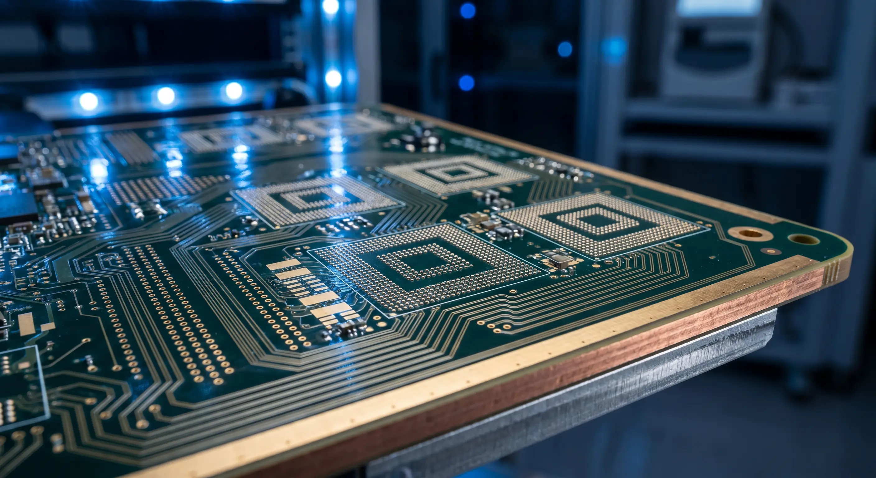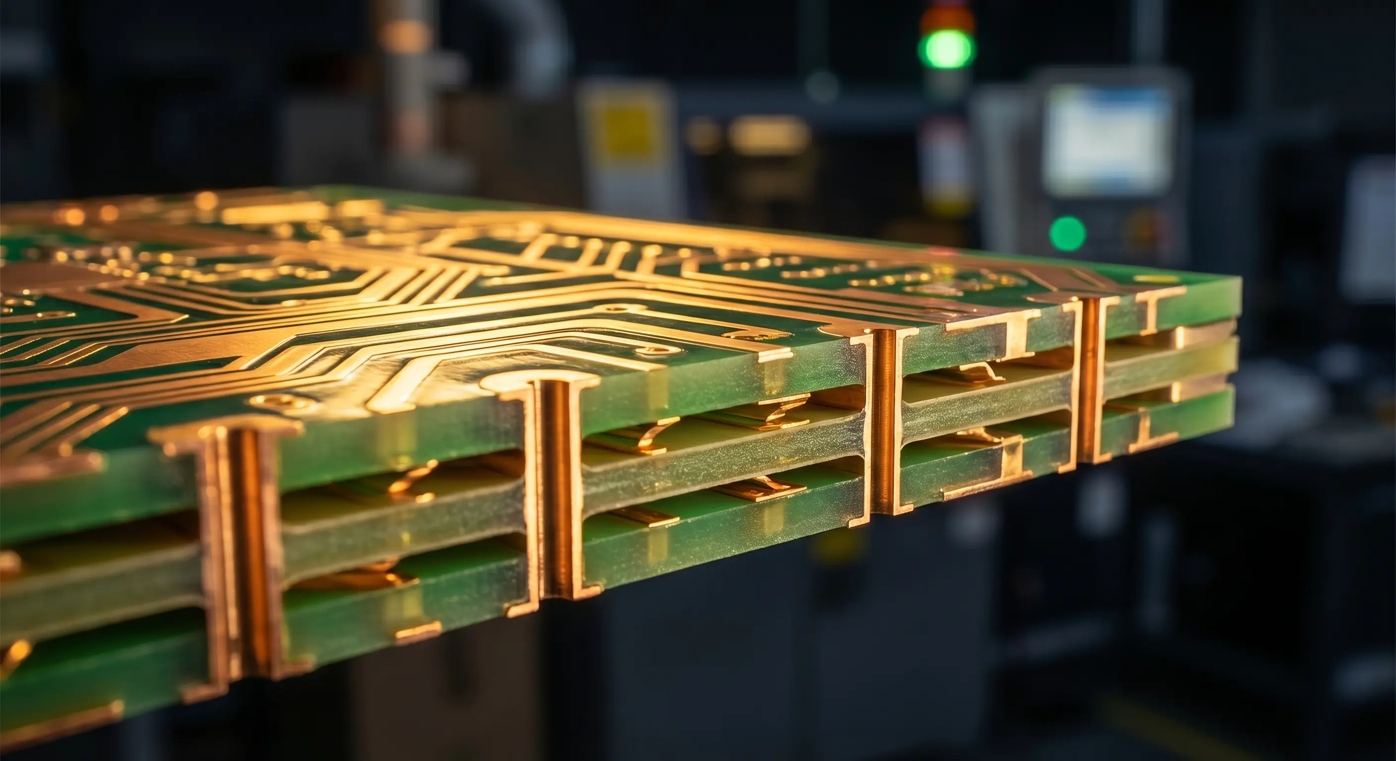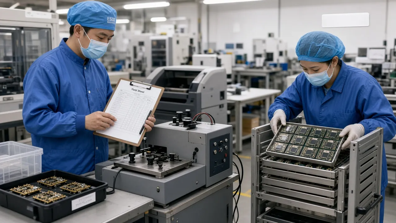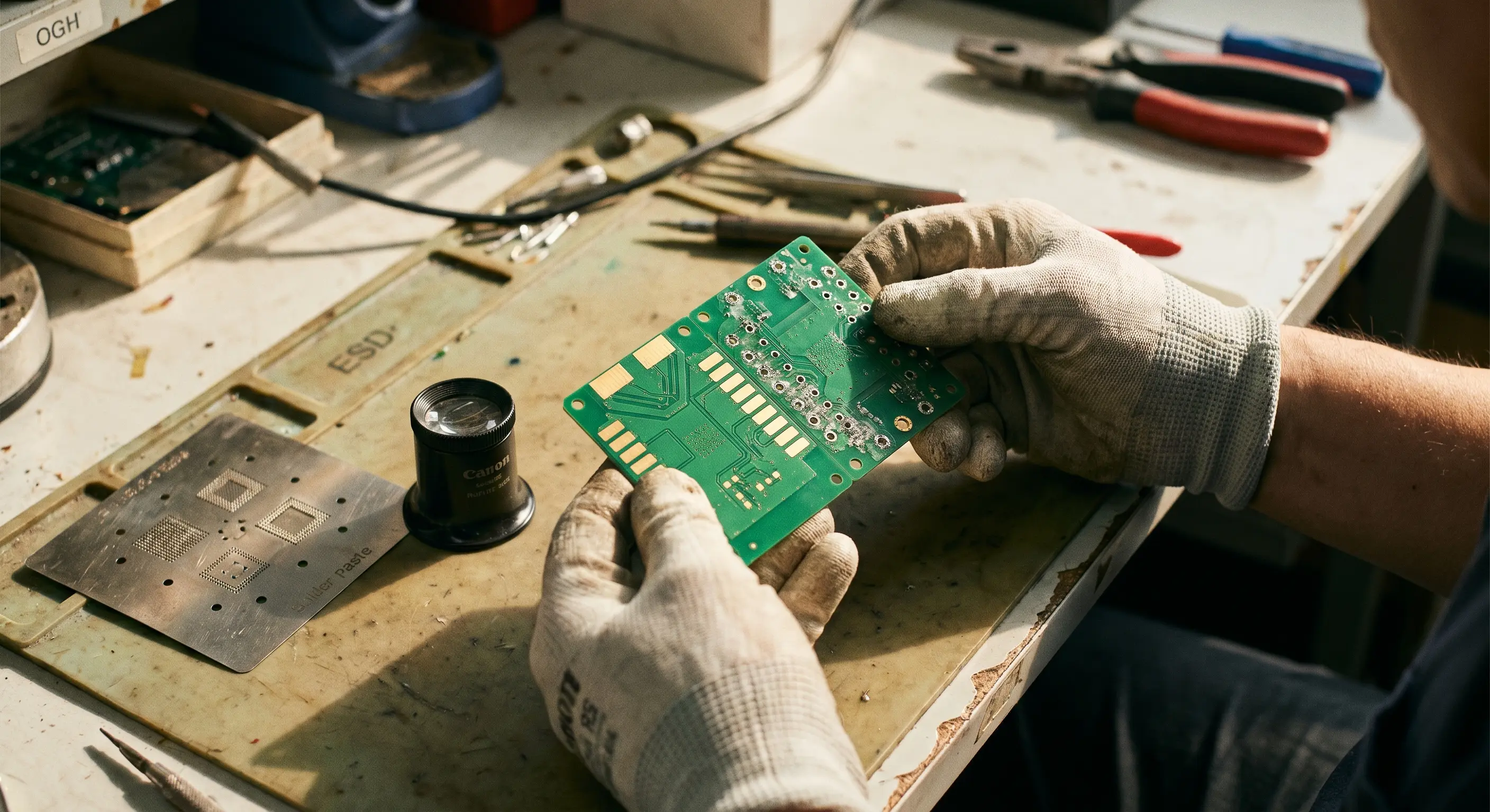
Choose the wrong PCB surface finish and your assembly yields drop, your BGA joints crack, and your boards fail in the field. The surface finish on exposed copper pads is far more than a protective coating — it determines solderability, pad flatness, shelf life, wire bonding capability, and whether your design survives multiple reflow cycles. With component pitches shrinking below 0.4mm and BGA ball counts exceeding 2000, the margin for error in surface finish selection has never been thinner. This guide breaks down every major PCB surface finish technology with real cost data, application rules, and a decision framework you can use on your next project.
What Is a PCB Surface Finish and Why It Matters
Bare copper oxidizes within hours of exposure to air. That thin oxide layer destroys solderability — the solder balls up instead of wetting the pad, creating cold joints or complete opens. A surface finish is a thin metallic or organic coating applied to all exposed copper pads after etching, protecting them until the assembly process.
But the finish does more than prevent oxidation. It directly impacts:
- Pad coplanarity — uneven finishes like HASL create height variations that prevent fine-pitch BGA solder balls from making contact
- Wire bondability — only certain finishes (ENIG, ENEPIG) support gold wire bonding for semiconductor packages
- Multiple reflow survival — double-sided SMT assemblies need finishes that survive two thermal cycles without degradation
- Test probe contact — ICT and flying probe fixtures need a durable surface that doesn't degrade under thousands of probe impacts
- RoHS compliance — lead-free mandates eliminated lead-based HASL in most markets, shifting the industry to alternative finishes
HASL (Hot Air Solder Leveling) — The Workhorse
HASL has been the default PCB surface finish for decades. The board is dipped into a bath of molten solder (now lead-free SAC305 alloy) and hot air knives blow off the excess, leaving a thin solder coating on all exposed copper. It's fast, cheap, and forgiving — which is why it still commands roughly 40% of the global PCB finish market.
Advantages
- Lowest cost — typically $0.05–$0.15 per board depending on size
- Excellent solderability — the pad is pre-tinned, so solder wetting is virtually guaranteed
- Long shelf life — 12+ months under proper storage conditions
- Robust for through-hole — thick solder coating fills through-hole annular rings reliably
- Multiple reflow capable — survives 3+ reflow cycles without degradation
Limitations
- Poor surface flatness — the hot air leveling process creates pad height variations of 5–15μm, unacceptable for fine-pitch BGAs below 0.5mm pitch
- Not suitable for HDI — uneven solder distribution causes co-planarity issues on micro-BGA and CSP packages
- Thermal shock risk — the 260°C solder bath can warp thin boards below 0.8mm
- Solder bridge risk — excess solder between fine-pitch pads requires careful process control
When to Specify HASL
Use HASL for general-purpose boards, power supplies, industrial controls, and any design with through-hole components and no fine-pitch BGAs. If your BGA pitch is ≥0.8mm and board thickness is ≥1.0mm, HASL is often the most cost-effective choice.
ENIG (Electroless Nickel Immersion Gold) — The Premium Standard
ENIG deposits two layers: a 3–5μm electroless nickel barrier over the copper, followed by a thin 0.03–0.08μm immersion gold layer. The nickel provides a diffusion barrier and mechanical base, while the gold protects the nickel from oxidation and provides excellent wire bonding and contact surfaces. ENIG is the second most popular finish globally and the default choice for high-density designs.
Advantages
- Perfectly flat surface — pad coplanarity within 1μm, ideal for fine-pitch BGAs, QFNs, and 0201/01005 components
- Excellent shelf life — 12–24 months, gold doesn't oxidize
- RoHS compliant — no lead, fully green
- Wire bondable — supports gold and aluminum wire bonding for hybrid assemblies
- Multiple reflow capable — nickel barrier survives 5+ reflow cycles
- Good for press-fit — hard nickel surface supports press-fit connector insertion
Limitations
- Higher cost — $1.00–$3.50 per board, 5–10x more expensive than HASL
- Black pad risk — improper nickel/gold process control can create phosphorus-rich layers that prevent solder wetting, causing catastrophic joint failures
- Signal loss at high frequency — nickel is ferromagnetic, causing 0.5–1.5 dB/inch additional insertion loss at frequencies above 10 GHz
- Complex process — requires tight chemical bath control and regular monitoring
When to Specify ENIG
Use ENIG for HDI boards, BGA-rich designs (especially below 0.5mm pitch), medical devices, aerospace applications, and any board that needs wire bonding or extended storage. ENIG is the safest choice when you can afford it — the flatness alone prevents a class of assembly defects that cost far more than the finish premium.
OSP (Organic Solderability Preservative) — The Budget Performer
OSP applies a thin organic compound (typically benzimidazole or phenylimidazole derivatives) directly onto bare copper. The film is only 0.2–0.5μm thick — virtually invisible — and dissolves into the solder flux during the first reflow cycle, exposing fresh copper for solder wetting. OSP is the lowest-cost flat finish available.
Advantages
- Very low cost — $0.05–$0.10 per board, comparable to HASL
- Perfectly flat surface — thinner than any metallic finish, excellent for fine-pitch SMT
- Environmentally friendly — no heavy metals, no toxic chemicals in waste stream
- Simple process — fast application, no complex chemical baths
- Good signal integrity — no nickel layer, no high-frequency loss
Limitations
- Very short shelf life — 3–6 months maximum, degrades rapidly in humid environments
- Poor multi-reflow performance — OSP degrades after the first reflow; double-sided assembly requires special handling
- No wire bonding — organic film cannot support wire bond connections
- Handling sensitivity — fingerprints and contamination destroy the OSP film; boards must be handled with gloves
- Not suitable for through-hole wave soldering — the OSP dissolves unevenly during wave solder, causing poor hole fill
When to Specify OSP
Use OSP for high-volume consumer electronics with single-sided SMT assembly, where boards go from fabrication to assembly within weeks. It's ideal for cost-sensitive smartphones, tablets, and IoT devices with fast inventory turns. Avoid OSP if your boards will be stored more than 3 months or require double-sided reflow.
Immersion Silver (ImAg) — The High-Frequency Compromise
Immersion silver deposits a thin (0.1–0.3μm) layer of pure silver onto copper through a galvanic displacement reaction. Silver offers excellent electrical conductivity and a flat surface at a moderate price point between OSP and ENIG.
Key Characteristics
- Cost: $0.30–$0.80 per board — 2–5x cheaper than ENIG
- Flatness: Excellent, comparable to ENIG
- Shelf life: 6–12 months (tarnishes if exposed to sulfur or high humidity)
- Best for: RF boards, high-speed digital (10+ GHz), signal-integrity-critical designs
- Watch out for: Tarnishing in storage, sensitivity to handling, not ideal for multiple reflows
Immersion Tin (ImSn) — The Press-Fit Specialist
Immersion tin deposits a thin (0.8–1.2μm) tin layer via chemical displacement. It's popular in European automotive manufacturing for press-fit connector applications, where the soft tin surface allows reliable press-fit pin insertion without damaging the PCB.
Key Characteristics
- Cost: $0.30–$0.70 per board
- Flatness: Excellent
- Shelf life: 6–12 months
- Best for: Press-fit connectors, automotive backplanes, European-specified designs
- Watch out for: Tin whisker growth over time, intermetallic growth with copper that degrades solderability after prolonged storage
Surface Finish Comparison Table
| Parameter | HASL | ENIG | OSP | ImAg | ImSn |
|---|---|---|---|---|---|
| Cost per board | $0.05–0.15 | $1.00–3.50 | $0.05–0.10 | $0.30–0.80 | $0.30–0.70 |
| Surface flatness | Poor | Excellent | Excellent | Excellent | Excellent |
| Shelf life | 12+ months | 12–24 months | 3–6 months | 6–12 months | 6–12 months |
| Fine-pitch SMT | ≥0.8mm | All pitches | All pitches | All pitches | All pitches |
| Through-hole | Excellent | Good | Poor | Good | Good |
| Reflow cycles | 3+ | 5+ | 1–2 | 2–3 | 2–3 |
| Wire bonding | No | Yes | No | No | No |
| RoHS compliant | Yes (LF) | Yes | Yes | Yes | Yes |
| High-freq loss | Low | Moderate | Very low | Very low | Low |
How to Choose: Decision Framework
Rather than memorizing specs, use this decision tree:
BGA pitch < 0.5mm?
→ ENIG or OSP. You need flatness. HASL's uneven surface will cause opens on fine-pitch BGA balls.
Storing boards > 6 months?
→ ENIG or HASL. OSP and ImAg degrade in storage. Long supply chains demand durable finishes.
High-frequency signals > 10 GHz?
→ OSP or Immersion Silver. Nickel in ENIG adds insertion loss at mmWave frequencies.
Press-fit connectors?
→ ENIG or Immersion Tin. Both support reliable press-fit insertion without pad damage.
Maximum cost pressure?
→ HASL for through-hole boards, OSP for SMT-only boards. Both are the cheapest options in their categories.
Medical or aerospace?
→ ENIG. Period. The reliability margin, shelf life, and traceability justify the cost.
Common Mistakes and How to Avoid Them
After reviewing thousands of PCB designs at Illuminious, these are the surface finish mistakes we see most often:
1. Specifying HASL on BGA boards below 0.5mm pitch
This is the single most common error. HASL's surface height variation of 5–15μm means some BGA balls sit on a solder dome while others land in a valley. The result: opens on the tallest pads, bridges on the shortest. The fix is simple — switch to ENIG or OSP for any design with fine-pitch BGAs.
2. Using OSP for double-sided assembly without planning
OSP degrades during the first reflow. When you flip the board for side B, the side A pads have lost their protection. If side A won't be reflowed again, this is fine. But if both sides need full solderability through two cycles, OSP will cause defects on the second pass. Solution: use ENIG for double-sided designs, or apply OSP only to side B while using ENIG on side A.
3. Ignoring shelf life in long supply chains
We've seen clients specify OSP for boards that sit in a warehouse for 8 months before assembly. OSP's 3–6 month shelf life means those boards arrive at the assembly line with degraded solderability, causing widespread wetting defects. Match your finish's shelf life to your actual supply chain timeline.
4. Not accounting for ENIG signal loss in RF designs
ENIG's nickel layer is ferromagnetic. At frequencies above 10 GHz, this introduces measurable insertion loss — sometimes 0.5–1.5 dB per inch of trace. For mmWave designs at 28 GHz or 77 GHz automotive radar, this loss is unacceptable. Use OSP or Immersion Silver instead.
What Illuminious Recommends
Our manufacturing engineers review surface finish specifications on every project. Here's our practical guidance based on the hundreds of designs we manufacture each month:
- Default choice: ENIG for anything with BGAs, fine-pitch components, or long supply chains. The cost premium is trivial compared to the assembly yield improvement.
- Budget option: Lead-free HASL for power supplies, motor controllers, and industrial boards with no fine-pitch components.
- High-volume consumer: OSP when you can guarantee assembly within 3 months of fabrication and single-sided SMT.
- RF and high-speed: Immersion Silver for the best combination of flatness, cost, and signal integrity.
- Automotive press-fit: Immersion Tin for European OEM requirements, ENIG for everything else.
The right surface finish is not about picking the most expensive option — it's about matching the finish characteristics to your specific design requirements, assembly process, and supply chain reality. Get this decision right, and you eliminate an entire class of manufacturing defects before they happen.
Need help selecting the right surface finish for your next PCB design? Our engineering team reviews every project with a detailed DFM analysis that includes surface finish recommendations based on your specific component mix and assembly requirements. Contact us to get started.