Advanced packaging has become the most critical frontier in semiconductor innovation. As Moore's Law slows and monolithic chip scaling delivers diminishing returns, the industry has pivoted to heterogeneous integration — combining multiple specialized die inside a single package to deliver performance that no single chip can match. The advanced packaging market is projected to surpass $65 billion by 2027, driven by AI accelerators, 5G modems, automotive processors, and edge computing devices. For hardware teams building next-generation products, understanding System-in-Package design and chiplet architecture is no longer optional — it is a competitive necessity.
Why Advanced Packaging Matters Now
The traditional approach to building faster chips — shrinking transistors and cramming more of them onto a single die — is hitting fundamental physical and economic walls. Wafer costs at 3nm and 2nm nodes exceed $20,000 per wafer, and a single defect on a large monolithic die can scrap an entire chip worth hundreds of dollars. Advanced packaging solves this by breaking large dies into smaller, more manufacturable pieces called chiplets, then reassembling them inside a single package with high-speed interconnects.
This shift creates enormous opportunities for hardware companies:
- Lower NRE costs: Chiplets can be designed, verified, and manufactured independently, reducing each design's complexity and time-to-market
- Higher yields: Smaller die sizes mean fewer defects per die — a 50mm² chiplet yields significantly better than a 400mm² monolithic die on the same process node
- Mix-and-match process nodes: Combine a 3nm compute chiplet with a 12nm I/O chiplet, optimizing cost and performance for each function
- Design reuse: A proven I/O chiplet can be reused across multiple product generations, amortizing development costs
- Faster iteration: Update only the chiplet that needs improvement rather than respinning an entire SoC
Key Advanced Packaging Technologies
1. System-in-Package
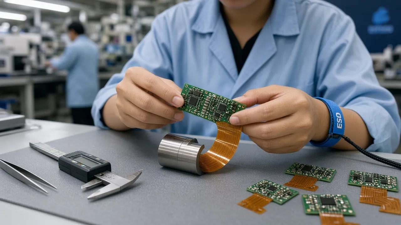
SiP integrates multiple ICs, passives, and MEMS devices into a single package. Unlike chiplets connected via high-speed interposers, SiP uses wire bonding, flip-chip, or embedded die techniques to create compact multi-function modules ideal for wearables, IoT, and mobile devices where space is critical.
2. 2.5D Interposer-Based
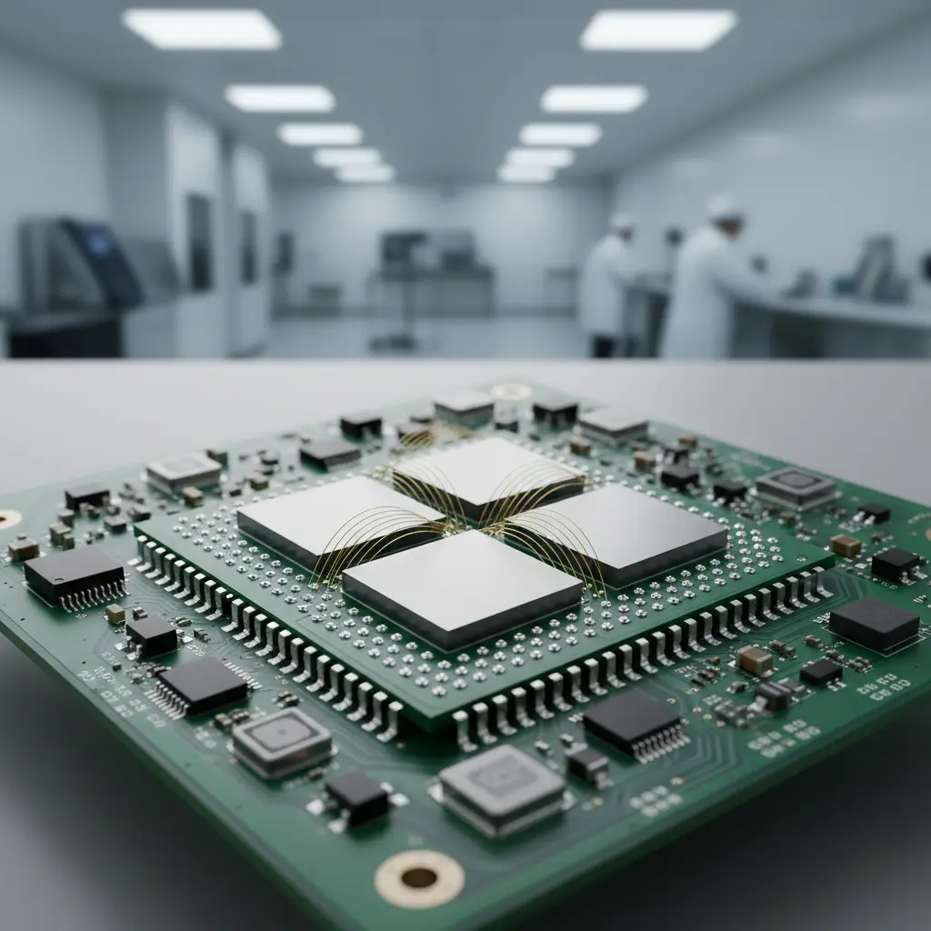
Die are placed side-by-side on a silicon or organic interposer with micro-bump pitches below 40μm. TSMC's CoWoS and Intel's EMIB are the leading platforms, enabling terabyte-per-second bandwidth between chiplets. This is the architecture behind NVIDIA's H100 and AMD's MI300.
3. 3D Stacked Die
Die are stacked vertically using through-silicon vias for vertical interconnect. TSMC's SoIC and Samsung's X-Cube enable logic-on-logic and logic-on-memory stacking with pitches below 10μm. 3D stacking delivers the highest bandwidth density but requires advanced thermal management.
4. Fan-Out Wafer-Level
FOWLP embeds die in epoxy mold compound and builds redistribution layers directly on the wafer, eliminating the need for a separate substrate. TSMC InFO is used in Apple's A-series and M-series processors, offering excellent electrical performance at lower cost than interposer-based approaches.
Die-to-Die Interconnect Standards
The chiplet ecosystem depends on standardized interfaces that allow die from different vendors to communicate reliably. Three standards are competing for dominance in 2026:
Universal Chiplet Interconnect Express is backed by Intel, TSMC, AMD, and ARM. It defines a physical and protocol layer for die-to-die connectivity at up to 32 GT/s per lane with support for CXL, PCIe, and AXI streaming protocols. UCIe is positioned as the universal standard for open chiplet ecosystems.
Bridge of Wire from the Open Compute Project targets simpler, lower-cost die-to-die connections using standard packaging substrates. It is well-suited for edge and IoT chiplets that do not require the extreme bandwidth of UCIe.
NVIDIA's NVLink-C2C and Apple's custom interconnects offer the highest performance but lock teams into a single vendor's ecosystem. These are appropriate when every gram of bandwidth matters and supply chain flexibility is secondary.
Interoperability Reality Check
While UCIe promises plug-and-play chiplet interoperability, the reality in 2026 is more nuanced:
- Physical layer compliance does not guarantee protocol-level compatibility
- Die from different foundries may require co-optimization of signal integrity
- Thermal and mechanical co-design between chiplets adds significant complexity
- Test and validation flows for multi-vendor chiplet systems are still maturing
Thermal and Mechanical Challenges
Stacking multiple heat-generating die inside a single package creates thermal management challenges that monolithic designs never faced. A 3D-stacked AI accelerator might need to dissipate 300-500W through a package smaller than a credit card. The thermal path from an upper die must pass through the lower die, creating thermal coupling effects that can push junction temperatures beyond safe limits.
- Thermal TSVs: Copper-filled through-silicon vias provide vertical heat conduction paths, but they consume die area and add manufacturing cost
- Micro-fluidic cooling: Direct liquid cooling channels etched into silicon interposers can remove 500W/cm² or more, enabling extreme 3D stacks
- Thermal interface materials: Advanced TIMs with thermal conductivity above 10 W/mK are essential for bridging gaps between die and heat spreaders
- Warpage management: Mismatches in CTE between silicon die, organic substrates, and mold compounds cause warpage during reflow — tolerances must stay below 50μm for reliable assembly
- Stress-aware layout: Die placement, underfill selection, and package substrate design must account for thermo-mechanical stress throughout the product lifecycle
Design-for-Packaging Best Practices
Transitioning from monolithic SoC design to chiplet-based systems requires new design methodologies and tool flows. Here are the practices that separate successful chiplet products from costly failures:
Partition Early
Define chiplet boundaries during architecture exploration. Functions with high internal bandwidth should stay on the same die. Only partition where the die-to-die bandwidth penalty is acceptable for your application.
Signal Integrity Co-Design
Simulate die-to-die links including the package substrate, interposer, and micro-bump parasitics. Eye diagrams must meet spec across process, voltage, and temperature corners.
Thermal Co-Simulation
Run coupled electrical-thermal simulations to identify hot spots early. Place high-power die adjacent to thermal TSVs and cooling channels. Never stack two high-power die directly.
Test Strategy
Design each chiplet with boundary scan and built-in self-test capabilities. Known-good-die testing before packaging assembly is critical — a single bad die can scrap the entire multi-chiplet package.
Supply Chain Flexibility
Source chiplets from multiple foundries where possible. Design your interconnect to tolerate minor timing variations between vendors. Avoid single-source dependencies on critical die.
Cost Modeling
Model the total cost of ownership including Known-Good-Die testing, advanced packaging assembly, yield loss at each step, and test coverage requirements. The packaging cost often exceeds the silicon cost.
Manufacturing and Assembly Considerations
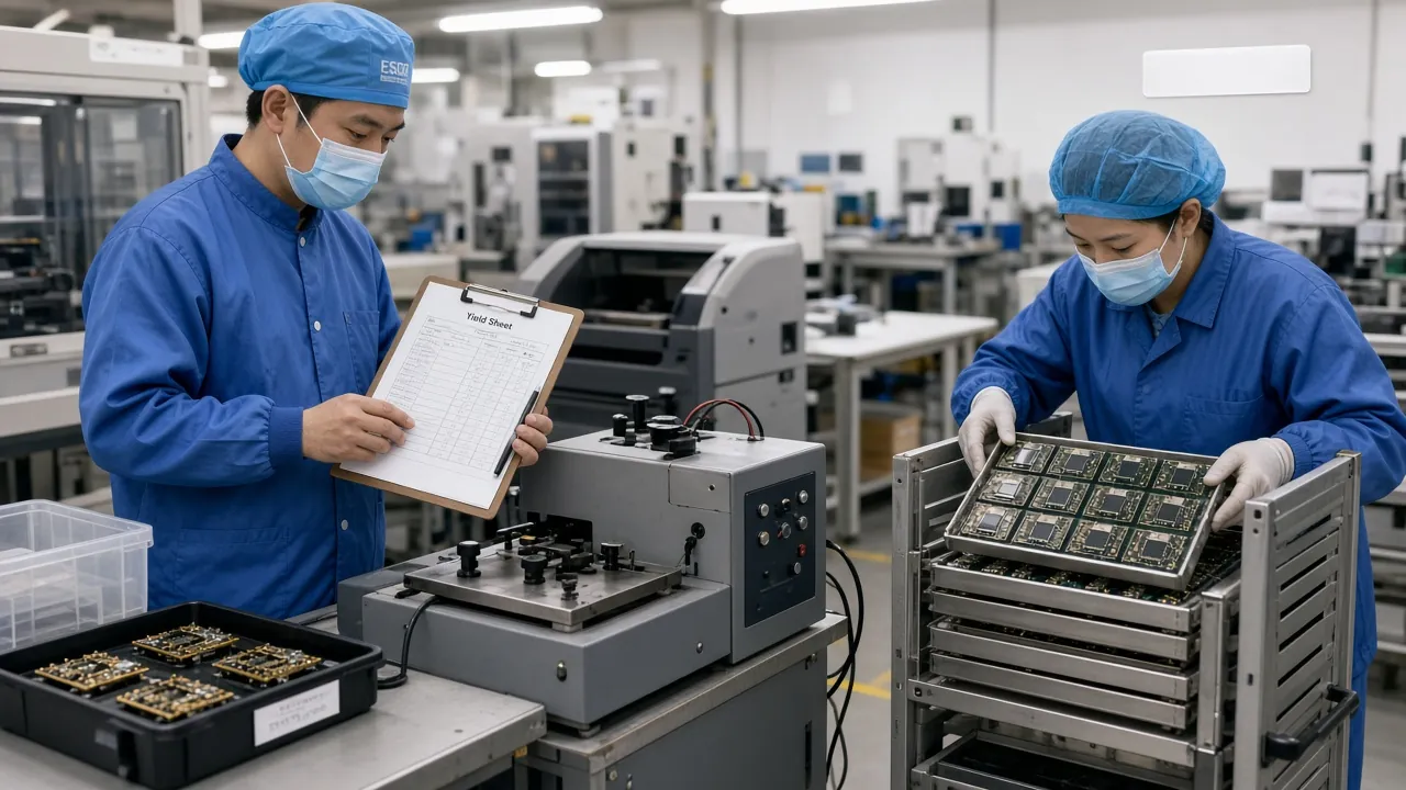
Advanced packaging assembly is fundamentally different from standard SMT. The processes require cleanrooms, precision placement equipment with sub-micron accuracy, and specialized metrology tools. Key manufacturing steps include:
- Known-Good-Die testing: Full functional and parametric testing of each bare die before packaging. KGD yield directly determines package yield — if each of 4 chiplets has 95% KGD yield, the package yield is only 81%
- Die placement and bonding: Flip-chip bonding at pitches below 40μm requires thermocompression bonding with forces measured in millinewtons and placement accuracy of ±1μm
- Underfill dispensing: Capillary underfill fills the gap between die and substrate, providing mechanical reinforcement and stress relief for micro-bump connections
- Warpage control: Mold compound selection, curing profiles, and process sequencing must minimize warpage to maintain assembly yields above 95%
- System-level test: After packaging, the complete multi-chiplet system must be tested as an integrated unit — defect localization across chiplet boundaries requires advanced test infrastructure
Illuminious Perspective
As advanced packaging adoption expands beyond hyperscale data centers into automotive, industrial, and consumer electronics, access to proven assembly and test partners becomes a strategic advantage. Illuminious works with hardware teams to navigate the complex ecosystem of OSAT providers, foundries, and packaging technologies — helping you select the right architecture for your product requirements and budget.
- End-to-end DFM review for advanced packaging designs
- OSAT partner matching based on technology requirements and volume
- Thermal and mechanical simulation support for chiplet-based systems
- Test strategy development from KGD screening to system-level validation
Looking Ahead: The Chiplet Ecosystem in 2027 and Beyond
The chiplet revolution is still in its early chapters. Several developments will shape the market over the next two years:
- Standardized chiplet marketplace: Platforms like the UCIe Consortium and DARPA's CHIPS program are building the foundation for an open chiplet marketplace where teams can license and integrate pre-verified die from specialized vendors
- Hybrid bonding maturity: Direct copper-to-copper bonding at pitches below 1μm will enable density increases of 10-100x over micro-bump connections, opening new possibilities for 3D integration
- Co-packaged optics: Integrating silicon photonics chiplets directly alongside compute die will eliminate the bandwidth bottleneck between processors and optical transceivers
- Automotive qualification: AEC-Q100 and ISO 26262 qualification of chiplet-based systems will enable advanced driver-assistance processors built from heterogeneous die
- Sustainability focus: Chiplet-based designs reduce semiconductor waste by enabling targeted replacement of only the obsolete die rather than scrapping entire monolithic chips
Advanced Packaging Is Your Next Competitive Edge
The companies that master advanced packaging and chiplet design will build faster, cheaper, and more flexible hardware products. The transition from monolithic thinking to heterogeneous integration requires new skills, tools, and partnerships — but the payoff is enormous.
Whether you are designing AI accelerators, automotive processors, or compact IoT modules, the right packaging strategy can be the difference between a product that leads and one that follows. Reach out to Illuminious to explore how advanced packaging can accelerate your next hardware project.